Quantcast
Channel: AnandTech Pipeline
Viewing all 3357 articles
Browse latest View live

Samsung Announces Tizen-based Gear 2, Gear 2 Neo Smartwatches

$
0
0

This morning Samsung dropped some news ahead of its Unpacked 5 event with the announcement of a refresh of its smart watch lineup, the Gear 2 and Gear 2 Neo. We reviewed the original Android 4.2 based Samsung Galaxy Gear, which offered an interesting combination of unique features in the smartwatch category (a strap mounted camera, Android platform, and bluetooth calling capabilities), but found that battery life left a lot to be desired partly thanks to it running the entire platform on an Exynos 4212. The new Gear 2 drops the "Galaxy" prefix and Android with it, instead opting for Samsung's own Tizen platform. Samsung doesn't call out an SoC specifically, but the Gear 2 is based on a dual core platform with maximum clocks of 1.0 GHz – previously Galaxy Gear was based on the dual core 4212 platform but with one core disabled and a maximum frequency of 800 MHz. The Gear 2 and Gear 2 Neo appear to be primarily differentiated by the presence of a body-mounted camera, with the 2 Neo eschewing the camera and likely coming in at a lower price point. 

  Galaxy Gear Gear 2 Gear 2 Neo
Display 1.63 inch 320x320 SAMOLED 1.63 inch 320x320 SAMOLED
SoC 800 MHz Exynos 4212 Dual Core Cortex A9 1 GHz "Dual Core"
OS Android 4.2 Tizen
Camera 2.0 MP w/AF 2.0 MP w/AF N/A
Video 720p30 720p30 N/A
Memory 4 GB + 512 MB RAM 4 GB + 512 MB RAM
Dimensions 36.8 x 56.6 x 11.1 mm, 73.8 g 36.9 x 58.4x 10.0 mm, 68g 37.9 x 58.8 x 10.0mm, 55g
Battery Li-ion 315 mAh Li-ion 300 mAh
Connectivity BT 4.0 Bluetooth 4.0, IrLED
Sensors Accelerometer, Gyroscope Accelerometer, Gyroscope, Heart Rate

The Gear 2 series adds some new functionality, including a heart rate sensor for health and fitness applications, IR led for controlling appliances with WatchOn, and the ability to change the wrist strap since the camera is now integrated into the body of the watch rather than on the strap. 

There also appears to be a hardware home button mounted below the display, although overall industrial design appears relatively unchanged from the original Galaxy Gear. Samsung also purports that battery life is now 2-3 days on the Gear 2, likely thanks to the change in software platform. Gear 2 will be available in April and we hope to get hands on with the watches as soon as possible.


MSI Launches the A88XI AC, a mini-ITX FM2+ 802.11ac Motherboard

$
0
0

Everyone likes the small and the powerful.  If I could get the power of a GTX Titan or R9 290X in a smartphone, we should all want one (in fact, how powerful are they compared to GPUs of yesteryear?).  For mainstream PC systems, mini-ITX is currently the form factor defining small, despite some attempts from VIA.  We have recently reviewed some small motherboards on the Intel side that can pack a punch, but MSI think its AMD A88X motherboard can do the same with a Kaveri APU.

The A88XI AC measures the mini-ITX spec of 17cm x 17cm, with support up to 32 GB of DDR3 via two DIMM slots.  The size of the APU socket is often a hindrance to mini-ITX boards and requires a special small form factor cooler, and MSI’s is done similarly to fit on the mini-PCIe slot, SATA ports and USB 3.0 header.  The CPU power connector is in an awkward position, underneath the power delivery heatsink which means that cables will have to stretch over the motherboard.

The 802.11ac is a dual band 2T2R solution from Intel, the Wireless-AC 7260 card.  This is paired with a Realtek ALC887 audio codec and Realtek Ethernet controller.  The audio controller was presumably chosen as it only requires three audio jacks on the rear IO, and MSI has placed fixed antenna positions on that rear panel.  The rear panel also contains two USB 3.0 ports, a VGA port, a DVI-D port and a HDMI port.

We have only two fan headers on board, but MSI have included a TPM header for the industries that need it.  Memory support is listed as both XMP and AMP up to DDR3-2133 MHz, and the PCIe x16 slot is Gen 3.0.

An additional feature in the press release for the A88XI AC is MSI's USB Power, which enables a cleaner power supply for the USB ports.  This should aid USB DACs in minimising power related noise issues.

The MSI A88XI AC should be available at retail in Q1.

MSI A88XI AC
Size mini-ITX
CPU Interface FM2+
Chipset AMD A88X (Bolton D4)
Memory Slots Two DDR3 DIMM slots supporting up to 32 GB
Up to Dual Channel, 1333-2133 MHz
Video Outputs VGA, 1920x1200 @ 60 Hz
DVI-D, 2560x1600 @ 60 Hz
HDMI, 4096x2160 @ 24 Hz, 3840x2160 @ 30 Hz, 1920x1200 @ 60 Hz
Onboard LAN Realtek RTL8111G
Onboard Audio Realtek ALC887
Expansion Slots 1 x PCIe 3.0 x16
1 x mini-PCIe
Onboard SATA/RAID 4 x SATA 6 Gbps (PCH)
USB 3.0 4 x USB 3.0 (PCH) [2 rear panel, 1 header]
Onboard 4 x SATA 6 Gbps
1 x USB 3.0 header
1 x USB 2.0 header
2 x Fan Headers
1 x Front Panel Connector
1 x TPM connector
Power Connectors 1 x 24-pin ATX Power Connector
1 x 4-pin CPU Power Connector
Fan Headers 1 x CPU (4-pin)
1 x SYS (4-pin)
IO Panel 1 x PS/2 Combination Port
1 x Optical SPDIF Output
VGA
HDMI
DVI-D
WiFi Antenna
4 x USB 2.0
2 x USB 3.0 (PCH)
1 x Ethernet (Realtek)
Audio Jacks (Realtek)
Warranty Period 3 Years
Product Page Link


Sapphire Combines the R7 250X with a Vapor-X Cooler

$
0
0

In order to differentiate yourself in the GPU market, a GPU vendor has to be creative and provide a feature that no-one else does.  On the high end cards, this is easier to perform, because a redesign of the power delivery, a better cooler, or a pre-overclocked GPU are often the tactics used.  When it gets down to the lower margin GPU parts, where the higher volumes are sold, it can be more difficult.  This is a segment where almost every cent counts.  Sometimes it pays to be the cheapest, and for various markets it is all about style or longevity.  To tackle this issue in the R7 250X space, Sapphire is releasing a model with their Vapor-X cooler.

The Sapphire Vapor-X R7 250X 1GB DDR5 OC is a dual slot card, featuring a core clock of 1100 MHz and 1300 MHz on the memory (5.2 GB/s effective).  The card is understandably dual slot, giving HDMI, DisplayPort, DVI-D and DVI-I connectors on the rear.  The 640 SPs are powered by a single 6-pin PCIe connector, and the box with the GPU will contain a 4-pin molex to 6-pin PCIe cable as well as a DVI to VGA adapter.  The listing online also states that the full retail SKU will also contain a 1.8 meter HDMI 1.4a cable, suitable for 3D viewing.

The Sapphire Vapor-X R7 250X 1GB DDR5 OC will be on sale shortly, although the MSRP has not been released.  The standard non-Vapor-X version of the GPU will also be available for $100, featuring slightly lower clocks (950 MHz core, 1125 MHz memory).

SanDisk iNAND Extreme in 2014: Finally a Good eMMC Solution for Mobile?

$
0
0

For the past couple of years we've been focusing more on tracking storage performance within smartphones and tablets. For the most part, we've come away disappointed. With smartphone ASPs trending downwards and many OEMs (other than Apple/Samsung) struggling to build healthy margins, internal storage is often leveraged as a high margin upsell and a cost optimized piece of the puzzle at the same time.

Sequential read/write performance has scaled reasonably well recently but random IO performance, particularly random write performance on a nearly full drive is very disappointing. With most devices incapable of more than a couple hundred random write IOPS, my recommendation to anyone has been to keep as much free space on your mobile device as possible in order to keep it feeling responsive. At MWC this week, SanDisk is offering another solution: a substantial step forward in high-end mobile eMMC performance.

Constrained by physical space limitations, smartphones and tablets typically leverage an integrated controller + NAND solution for storage. In some cases, a big silicon player may have an SSD controller on their applications processor and simply connect it to dumb, external NAND (e.g. the Apple approach). A lot of the time we just see a single-chip eMMC solution that integrates an eMMC controller and NAND.

SanDisk is a popular provider of these highly integrated mobile solutions, and is announcing the latest update to its iNAND Extreme family.

We're once again talking about a single-chip eMMC+NAND solution, but one that's much faster than previous incarnations. All implementations use SanDisk's own 1Y nm 2-bit-per-cell MLC NAND. In the new iNAND Extreme, SanDisk moves to a dual-CPU (one core for host operations and one for NAND management), dual-channel design. Multiple cores are common in high-end SSD controllers, so it's good to see mobile focused designs maturing to the same point.

The new iNAND Extreme implements eMMC 5.0 with a 400MB/s host interface. Internal to the design however are two 300MB/s channels connecting the controller and NAND. The bandwidth mismatch is designed to allow the device to work quicker internally to hide garbage collection and other cleanup latencies from the end user.

The old iNAND Extreme, much like most of the other eMMC solutions on the market today, was designed with a block based mapping architecture optimized for high sequential performance but low random IO performance. With the new iNAND Extreme, SanDisk moves to a page mapped architecture that has a significant impact on random IO performance as you can see in the table below. SanDisk does a pretty good job of dirtying its drives before running performance tests. Each drive is filled multiple times and around 10% of the drive is kept clean to simulate a heavy, real world use case. If SanDisk's testing description is indeed accurate, then the numbers below should be representative of what you'd experience on your phone/tablet:

SanDisk iNAND Extreme 2014 Update
  16GB 32/64GB
Random Read Performance 6K IOPS 6K IOPS
Random Write Performance 3K IOPS 3K IOPS
Sequential Read Performance 300MB/s 300MB/s
Sequential Write Performance 40MB/s 80MB/s

The new iNAND Extreme uses 64Gbit MLC NAND die and at launch will be available in 16GB, 32GB and 64GB variants. SanDisk will eventually follow up with a 128GB variant with a whopping 16 NAND die on a single package.

Although the new iNAND Extreme has two NAND channels, it's possible to interleave requests to multiple die on each channel and thus we see a benefit to having more than 1 die per channel. Sequential read speeds are absolutely phenominal on the new iNAND Extreme. At 300MB/s we're not far off where full blown SATA SSDs were just a couple of years ago. Sequential write speeds have improved tremendously as well. At 80MB/s for the 32/64GB drive, we're talking about multiple times faster writes than what we see in leading phones/tablets today.

The big win is in the random IO performance. SanDisk tests with 4KB transfer sizes and at 3K IOPS we're talking about around 12MB/s of random write performance. While steady state random write performance on many eMMC solutions in use today isn't much better than a high end 3.5" hard drive, the new iNAND Extreme should manage to deliver an order of magnitude better performance. Random read performance is also great.

I've seen SanDisk's iNAND solutions used in Chromebooks before. It's not clear to me what's kept it out of a lot of the phones we typically review. I am also very curious about the power consumption, but SanDisk is aiming for everything from high end smartphones and tablets to notebooks with the iNAND Extreme so it had better be fairly low power.

Needless to say I'm extremely excited to see an eMMC solution offer this level of performance. We've seen tremendous progress on CPU, GPU and connectivity fronts in mobile over the past few years, it's about time we saw the same with storage.


Audience Announces MQ100 Motion Processor

$
0
0

Just a few weeks ago, Audience announced its fourth generation of voice processors at CES, which added an always-on voice activation feature called VoiceQ designed to enable experiences similar to the "OK Google" feature on the Moto X. Today Audience is announcing a product for an entirely different segment, the MQ100 always-on sensor hub with sensor fusion utilizing the same proprietary DSP architecture it developed for its eS line of voice processors. 

Audience's positioning for the MQ100 is clever – combining inputs from accelerometer, gyro, and other sensors makes it analogous to an inner ear, not far off from the cochlear functions its says it can emulate in its voice processors. The MQ100 is built on the same 40nm process as the rest of the eS series, and uses the same ISA. It's capable of doing 9-axis sensor fusion at under 5 mW peak, and around 1 mW average, which it says is lower than the 10-20 mW from similar designs using either straight ARM IP or competitor fixed-point DSPs (Audience's DSP architecture is floating point and SIMD). Audience isn't developing its own sensor fusion software, but rather opening up its ISA to software partners to port their algorithms over, and will supply the necessary drivers for sensors that plug into it. 

In addition, the same motion processing software will be available in the eS line of voice processors, rounding out the curious gap in product numbering that we saw earlier with the new MotionQ enabled combinations. Audience expects samples of MQ100 in Q2 2014. 

Qualcomm's Snapdragon 801 (MSM8974AC): The New 32-bit Flagship Until 805

$
0
0

As Qualcomm continues to move its SoCs to 64-bit ARMv8 based cores, there's still demand for high-performance 32-bit solutions today. We're still some months away from Snapdragon 805 showing up in devices, but the next generation of Android flagships is getting ready for announcement at MWC this week. To satiate the needs of its high end customers, Qualcomm is shipping a higher clocked variant of the MSM8974/Snapdragon 800 called the Snapdragon 801 (MSM8974AC).

Architecturally the SoC is identical to its namesake. The Snapdragon 801 features four 32-bit Qualcomm designed Krait 400 cores and an Adreno 330 GPU. The DSP and ISP blocks haven't changed either. And we're still talking about a 2 x 32-bit LPDDR3 memory interface. What is different are the frequencies all of these blocks operate at. The differences are in the table below:

Qualcomm Snapdragon 800 vs. 801
  MSM8974 (Snapdragon 800) MSM8974AB (Snapdragon 800) MSM8974AC (Snapdragon 801)
CPU 4 x Krait 400 4 x Krait 400 4 x Krait 400
Max CPU Frequency 2.3GHz (2.26GHz) 2.3GHz (2.26GHz) 2.5GHz (2.45GHz)
GPU Adreno 330 Adreno 330 Adreno 330
Max GPU Frequency 450MHz 550MHz 578MHz
ISP Frequency 320MHz 465MHz 465MHz
Memory Interface 2 x 32-bit LPDDR3-1600 2 x 32-bit LPDDR3-1866 2 x 32-bit LPDDR3-1866
eMMC Interface 4.5 4.5 5.0
Modem 9x25 IP block, Category 4 LTE 9x25 IP block, Category 4 LTE, DS-DA 9x25 IP block, Category 4 LTE, DS-DA

Max CPU frequencies go up by around 8%. I put Qualcomm's official numbers in parantheses next to the numbers that are usually quoted for these parts in marketing materials. Max GPU frequency goes up by a substantial 28%, and the peak theoretical memory bandwidth goes up by 16%. Given that most mobile GPU benchmarks tend to be shader rather than memory bandwidth bound, Snapdragon 801 should do quite well in the usual metrics.

Moving to eMMC 5.0 enables support for up to a 400MB/s interface, which we'll see used by new eMMC solutions like the latest iNAND Extreme from SanDisk. The Snapdragon 801 retains a similar MDM9x25 derived modem IP block with support for Category 4 LTE, while adding support for DS-DA (dual-sim, dual-active).

You should expect to see the Snapdragon 801 used many of the major flagship smartphones announced at MWC this week.

Snapdragon 610 & 615: Qualcomm Continues Down its 64-bit Warpath with 4/8-core Cortex A53 Designs

$
0
0

The unexpected arrival of Apple's first 64-bit ARMv8 core (codename: Cyclone) at the end of last year forced a transition to 64-bit sooner than expected. Silicon vendors keep telling me that both quad-core and 64-bit support are now borderline requirements for customers in China. I'm still skeptical that the Chinese market wouldn't respond just as well to a really well designed, high performance dual-core 32-bit SoC, but since there isn't one on the market we'll never really find out.

In order to quickly respond to market demand for 64-bit and tons of cores, Qualcomm is bringing ARM's own IP higher up the product stack into the new Snapdragon 610 and 615. Both SoCs are being announced at MWC, with shipments to customers in Q3 and the first devices hitting the market sometime in Q4 of this year.

The Snapdragon 610 and 615 are four and eight core implementations of ARM's Cortex A53, combined with Qualcomm's Adreno 405 GPU and the company's own 9x25 derived Category 4 LTE modem. The SoCs are built on a 28nm LP process, like the Snapdragon 410. The two new SoCs are also pin compatible with the Snapdragon 410, offering phone vendors an easy way of designing a higher performance version of a 410 platform.

That's the high level take, now let's dig a bit deeper.

New to the Roadmap: 64-bit and Octa-core

Like the Snapdragon 410, both the 610 and 615 use ARM's 64-bit Cortex A53 CPU IP. The main difference between the two SoCs is the number of cores. The 610 features four Cortex A53s, while the Snapdragon 615 features eight. Qualcomm readily admits that the Snapdragon 615 exists almost entirely because of the China market. I really do wonder if both the 610 and 615 have eight CPU cores with four fused off to make a 610, as creating two separate masks/die at this price point may not make a ton of sense.

Qualcomm's Growing 64-bit SoC Lineup
Marketing Name Snapdragon 615 Snapdragon 610 Snapdragon 410
Internal Model Number MSM8936 MSM8939 MSM8916
Manufacturing Process 28nm LP 28nm LP 28nm LP
CPU 8 x ARM Cortex A53 4 x ARM Cortex A53 4 x ARM Cortex A53 1.2GHz+
ISA 32/64-bit ARMv8 32/64-bit ARMv8 32/64-bit ARMv8
GPU Qualcomm Adreno 405 Qualcomm Adreno 405 Qualcomm Adreno 306
H.265 Decode Yes Yes No
Memory Interface 1 x 64-bit LPDDR2/3 1 x 64-bit LPDDR2/3 1 x 64-bit LPDDR2/3
Integrated Modem 9x25 core, LTE Category 4, DC-HSPA+, DS-DA 9x25 core, LTE Category 4, DC-HSPA+, DS-DA 9x25 core, LTE Category 4, DC-HSPA+, DS-DA
Integrated WiFi Qualcomm VIVE 802.11ac Qualcomm VIVE 802.11ac Qualcomm VIVE 802.11ac
eMMC Interface 4.5 4.5 4.5

I briefly went over the architecture of ARM's Cortex A53 in my post on the Snapdragon 410. In short, it's a 64-bit ARMv8 Cortex A7 on steroids. ARM views the Cortex A53 as the absolute furthest you can push a dual-issue, in-order microprocessor. It's going to make for an excellent performer in the mainstream.

Both SoCs are built on a 28nm LP process. The 8-core Snapdragon 615 is made up of two quad-core clusters, each optimized for a different operating point. One cluster is optimized for low power operation while the other cluster is optimized for high performance. This will likely manifest in four cores being able to run at a higher frequency than the other four, although Qualcomm tells me that all eight cores can be operational at the same time should a workload demand it. More likely than not we'll see situations where you have either the low power or high performance cluster operational, and not both. There simply aren't many (any?) normal use cases where you need 8 active cores. 

This dual-cluster approach should sound a lot like NVIDIA's 4+1 architecture. While the Snapdragon 615 meets the core count requirements for success in China, it also offers a bit more dynamic range for regular users as well.

I do have to point out that the Snapdragon 615 violates Anand Chandrasekher's Things that are Dumb list, but again it seems like Qualcomm is simply doing what the Chinese OEMs want. I could have a longer discussion about whether or not it's smart to listen to your customers if they are leading you astray, but let's see how this one pans out once Qualcomm shifts back over to its own CPU core IP next year. 

The big upgrade over the Snapdragon 410 actually comes on the GPU side as both the 610/615 integrate Qualcomm's Adreno 405 GPU. It's unclear how Adreno 405 compares, performance-wise, to Adreno 420 in the Snapdragon 805 but we do see a substantial feature set increase with the move to a 4xx GPU. Qualcomm's Adreno 400 GPU family is designed in house and brings a D3D11-class feature set to Qualcomm's mobile SoCs. There's support for hardware tessellation, DirectX 11.2, OpenGL ES 3.0 and full profile OpenCL 1.2.

I don't have many details about the ISP, but Qualcomm tells me to think of the 610/615 as bringing features down from the Snapdragon 800 family rather than bringing features up from the 410. The 610/615 also add hardware HEVC/H.265 decode acceleration.

The Snapdragon 410, 610 and 615 all have the same pinout, which implies that they all have the same 64-bit LPDDR2/LPDDR3 memory interface.

Connectivity and Conclusion

On the modem front all three 64-bit SoCs integrate Qualcomm's 3rd generation LTE, basically a derivative of the 9x25 core that we've seen used for a while now. There's support for Category 4 LTE and optional Carrier Aggregation. The new 610/615 are compatible with Qualcomm's RF360 front end, which we expect to see fully deployed and available in a device by the end of the year. Continuing with Qualcomm's tradition, the new SoCs also integrate its 802.11ac WiFi.

Given Qualcomm's very public statement against 8-core mobile CPUs back in August of 2013, I can only assume that the 8-core Snapdragon 615 is a very new addition to the roadmap. I do wonder what might've filled this space had Apple not released the A7 when it did. I also wonder what the 64-bit successor to the Snapdragon 805 will be. It's too early for Cortex A57 but I wouldn't rule that out for a future 800 series Snapdragon SoC.

The Snapdragon 610 and 615 appear to fulfill Qualcomm's desires for bringing 64-bit designs to market as quickly as possible, as well as the need to compete in the core count race in China. I don't agree with either philosophy, but I'm also not tasked with selling SoCs on a global scale - perhaps this is the only way. It also highlights a serious weakness in ARM's roadmap: anyone looking to build a 64-bit performance mainstream SoC is forced into tons of low power cores rather than fewer, higher IPC cores. We need a 64-bit version of the Cortex A17.

I do wonder how the Cortex A53 will measure up to Krait 300. The latter isn't incredibly out-of-order, but it can run at relatively high frequencies. Since we're talking about 28nm LP designs, I'm not expecting super high frequencies out of Cortex A53. This may be one of the few times in recent history where we get to pit ARM's own design against a similar, competing solution from Qualcomm.

Moving the needle on graphics is important and it's good to see quick progress on that front. I suspect both of these SoCs will make for good midrange devices.

ZTE Announces Use of Qualcomm CMOS PA as March Towards RF360 Continues

$
0
0

Today at MWC Qualcomm announced ZTE will be the first smartphone customer to ship with Qualcomm's CMOS Power Amplifier, a part of its RF360 front end solution. This is a very big deal. We somehow missed covering the RF360 announcement in great detail last year, so I'm going to quickly recap it here first.

We often talk about two major parts of the cellular connectivity story in our reviews: the cellular modem and transceiver. The diagram below does a good job of illustrating the chain:

In front of the transceiver you have antennas, switches, band filters and power amplifiers. Each band you need to support has a filter, power amp (PA) and antenna switch. In the old days it was one PA per band but now you can have multiple bands handled by a single PA. All of these components consume power and take up board area. More importantly, as you want to support more bands in a single device you need to scale up the number of switches, filters and PAs, which in turn consumes more board area. Larger PCBs lead to larger devices, which isn't always desirable.

Qualcomm's RF360 front end is an attempt to consolidate everything ahead of the transceiver in order to reduce power consumption, board area and enable support for more bands in a single device. While mobile operators may fight over limiting what bands are enabled on their devices, being able to support more in a given board area is incredibly useful from a manufacturing perspective. Smartphone vendors want to build as few SKUs as possible to service the world.

So what is Qualcomm's RF360? The front end is comprised of four parts: the QFE11xx Envelope Power Tracker, QFE15xx Dynamic Antenna Matching Tuner, QFE23xx Integrated Power Amp and Antenna Switch, and QFE27xx RF PoP.

The envelope tracker (QFE1100) was deployed in Samsung's Galaxy Note 3, Nexus 5, and in an APT (Average Power Tracker) mode in the LG G2 (QFE1101), and helps reduce power consumption/thermal footprint by dynamically varying voltage across the PA depending on the waveform of the transmitted signal (instead of leaving it as a fixed value).

The dynamic antenna matching tuner showed up in Nokia's Lumia 1520 and actively tunes attached antennas depending on current conditions. The next piece of the RF360 puzzle is the QFE23xx power amp. This is a 28nm power amp built in CMOS at a 28nm process, which moves conventional front end analog circuitry into a smaller, scalable CMOS package. The CMOS power amp needed quite a bit of validation/field verification testing, which contributed to a fairly long time to market. Today Qualcomm announced that ZTE is its first partner to design in its QFE23xx CMOS power amps with the new Grand S II LTE.

ZTE uses two Qualcomm CMOS power amps in its design (QFE2320, QFE2340), in addition to Qualcomm's QFE1100 envelope tracker.

The last piece of the RF360 puzzle is the QFE27xx RF PoP. This is a package-on-package design that takes the CMOS power amps, and moves the band filters off of the PCB and onto the power amp itself, thereby reducing board space. Qualcomm expects to see the first full RF360 implementation in a smartphone later this year (likely about a quarter after today's announcements).

The benefits are obvious. Reducing board area and power consumption has a direct impact on the size, weight and battery life of a device. Smaller PCBs can be leveraged to either build smaller devices, or support more bands while keeping the device size the same. It's wonderful to see Qualcomm being more aggressive in talking about its connectivity wins, and I'm very excited to see that RF360 is nearly completely here. This is a very big deal.


Sony Launches Xperia Z2, Z2 Tablet, and M2 at MWC 2014

$
0
0

Sony Xperia Z2

Sony has just announced the Xperia Z2, which is the direct successor to the Xperia Z1 that released in the fall. While quite a bit stays the same, there’s also quite a bit that has changed. I’ve listed the differences below:

  Sony Xperia Z1 Sony Xperia Z2
Display 5”, 1080p “Triluminos” display 5.2”, 1080p “Triluminos” display
Video Recording 1080p 2160p/4K
SoC MSM8974, 2.15 GHz Snapdragon 800 MSM8974AB 2.26GHz Snapdragon 800
RAM 2 GB 3GB
Speakers Single speaker, downward-facing Stereo speakers, front-facing “S-Force Front Surround”
Battery  3000 mAh, 3.8V, 11.4 WHr 3200 mAh, 3.8V, 12.16 WHr

While there’s plenty of other things mentioned in the press release, much of it is the standard fluff and fanfare that most press releases come with. Ultimately, the differences come down to the spec sheet, and the Xperia Z2 has few notable changes from the Xperia Z1. Battery gets larger to compensate for the larger display, Sony added the ability to record in 4K/30p, the SoC is a minor bump from improved yields, RAM goes up to compete with Samsung’s Note 3 and presumably a future Galaxy S phone as well.

While I will admit that I haven’t properly used either Xperia Z1/Z2, I do have a good idea of the various issues that seem to be consistently repeated by Sony in their Xperia lineup. Probably the biggest question that I have is whether the Xperia Z2 truly has a better display than the Xperia Z1. While the press release talks about how “TRILUMINOS Display for mobile with brand new Live Colour LED uses red & green phosphor with blue LEDs and customised colour filters to produce a brighter and more uniform light. The result is richer colours on the screen for all of your smartphone viewing without the risk of saturation,” I am skeptical that this actually translates to better display. While it’s too early to judge whether display has truly changed from the Z1’s display with poor calibration and worse viewing angles, initially it seems that nothing significant has changed.

What can be talked about is the MSM8974AB, a SoC that was already outed by Xiaomi with their Mi-3. The differences are minor, far smaller than that of the APQ8064 and APQ8064AB/AC, which had slightly improved IPC and higher clocks. The 8974AB instead brings higher GPU clocks (550 MHz vs 450 MHz), higher memory clocks (933 MHz vs 800 MHz), and the ISP goes from 320 MHz to 465 MHz. This is almost guaranteed to be the SoC of choice for all high end flagships launching at MWC, judging by various rumblings about the internet.

The final change of note in the Xperia Z2 are the stereo front facing speakers, which are finally in a phone that doesn’t start with One or Butterfly in the model name. While there aren’t many details on the quality of the speakers, just putting them on the front is great. However, just like with HTC devices, it seems that the speakers have added a great deal of bezel to the front of the device. While some may not mind the difference, there are definitely a great deal of people that voice their complaints over the size of bezels in phones.

Outside of hardware, it should be noted that Sony is advertising a “built-in noise cancelation feature with certain earbuds. These would use two microphones located on the earbuds and leverage the smartphone for the noise cancelation processing.

Sony Xperia Z2 Tablet

Following up Sony’s launch of the Xperia Z2, they’ve also launched the Xperia Z2 tablet, which fits the name well, as it is effectively has the same internals as the Xperia Z2, only made into a tablet, which means removing the data/voice modem for the Wi-Fi variant, increasing the screen size to 10.1”, and changing the camera from the 20.7MP, 1/2.3” sensor found in the Xperia Z2 to an 8.1MP unit on the back, likely of either 1/4” or 1/3” format. There are some changes to battery size, thickness, and weight, but everything else is carried over, such as the FHD Triluminos display, IP55/58 rating and the front-facing stereo speakers.

                The rest of the specs and the press release can be seen below:

  Sony Xperia Z2 Tablet
Display 10.1”, 1080p “Triluminos” display
SoC MSM8974AB (LTE) APQ8074 (WiFi), 2.26 GHz Snapdragon 801
RAM 3 GB
Rear Camera 8.1MP, Exmor RS for Mobile
Front Camera 2.2MP
Thickness 6.4mm
Mass 426g (Wi-Fi), 439g (LTE/3G)

Sony Xperia M2

Finally, Sony launched the Xperia M2, a mid-range device that seems to directly target the Moto G based upon its platform and spec. I say this because the SoC is the Snapdragon 400 with quad core Cortex A7s at 1.2 GHz. The one major difference is that this phone has LTE. This means that it’s probably the MSM8926 running inside, unless Sony is packaging a separate modem to enable LTE, which is rather unlikely. Of course, specs always form the foundation of experience for a device, which can be seen below

  Sony Xperia M2 Moto G
Display 4.8" qHD 4.5" 720p
SoC MSM8926, Quad Core 1.2 GHz Cortex A7 MSM8226, Quad Core 1.2 GHz Cortex A7
RAM 1 GB 1 GB
Rear Camera 8MP, Exmor RS for Mobile 5MP
Storage 8 GB 8/16 GB
Thickness 8.6mm 6-11.6mm

This is an interesting device because it’s not a simple refresh. The display is likely to not be competitive with the Moto G unless its calibration is much better, but Sony has also introduced LTE into their device. The camera could be noticeably better, as the 5MP camera in the Moto G is certainly not targeted at anyone that intends to use their phone as a primary camera of any kind. The Xperia M2 also has a dual-SIM variant, although that device won’t have LTE. While the press release doesn’t have any indication of whether or not the Xperia M2 will have microSD, it should be a relatively safe bet to say that it will, based upon Sony’s continued inclusion of microSD even at the high end of the market. Overall, depending upon price, this will be competitive with the Moto G, as they trade blows in specifications.

Imagination's PowerVR GX6650: Competition for Mobile Kepler

$
0
0

Ryan touched on this in his excellent deep dive on Imagination's PowerVR Series 6XT GPU architecture earlier today, but I wanted to specifically call out the new high-end from IMG that was announced back in January. Pictured above is a high-level block diagram of the new PowerVR GX6650, this is IMG's answer to NVIDIA's mobile Kepler/Tegra K1

Below I've included a modified version of Ryan's comparison table from his architecture piece:

GPU Specification Comparison
  NVIDIA K1 Imagination PowerVR GX6650 Imagination PowerVR G6430 Imagination PowerVR G6230
FP32 ALUs 192 192 128 64
FP32 FLOPs 384 384 256 128
Pixels/Clock (ROPs) 4 12 8 4
Texels/Clock 8 12 8 4
GFLOPS @ 300MHz 115.2 GFLOPS 115.2 GFLOPS 76.8 GFLOPS 38.4 GFLOPS
Architecture Kepler Rogue (Series 6XT) Rogue (Series 6) Rogue (Series 6)

I tossed in the Series 6 PowerVR G6430 as a comparison point. The G6430 is the GPU in the iPad Air/iPad mini with Retina Display/iPhone 5s. If Apple decides to go all out with a GPU upgrade on its next-generation iPad Air (A8/A8X silicon perhaps?), the GX6650 would likely be the IP to use. 

Intel Talks Atom Z3460/Z3480 (Merrifield), Z3560/Z3580 (Moorefield) and LTE at MWC 2014

$
0
0

For the past couple of years Intel has used MWC as an opportunity to update us on its mobile plans. This year is no different as Intel officially launches its latest LTE modem and first 22nm smartphone SoC.

Intel is announcing their 2nd generation multi-mode LTE modem at MWC: the XMM 7260. Brian already went through and did a great job explaining what the 7260 is and what it's capable of in his article from last year. In short, the XMM 7260 is Intel's first category 6 LTE modem with support for carrier aggregation. The 7260 is paired with Intel's SMARTi 45 transceiver that enables single-chip CA. On paper the 7260 is a competitor to Qualcomm's forthcoming 9x35 modem, however it's built on TSMC's 28nm process compared to the 20nm node that Qualcomm is using for 9x35. Intel claims its architecture is extremely power efficient despite the foundry disadvantage (an admittedly unusual position for Intel to be in). It will take Intel 2 - 3 years to bring its modem manufacturing in-house.

The XMM 7260 is presently going through certification at tier 1 mobile operators and Intel expects devices on shelves in Q2 of this year.

The XMM 7260 is a very important product for Intel as it hopes to put a dent in Qualcomm's almost exclusive dominance of the LTE space. By the end of 2014 Intel hopes to be the obvious second choice behind Qualcomm. While it's not incredibly common to talk about pricing, I suspect that's going to be an advantage that Intel hopes to exploit over Qualcomm. As the new comer (at least to LTE) with everything to prove, I'd expect Intel to offer XMM 7260 at a discount to what Qualcomm charges for its alternatives. Intel being the value player may be unique in its silicon business, but it's not unique in its role in mobile thus far. The 3G XMM 6260 was widely used by many OEMs as it was an incredibly reliable, and cost-effective solution. As growth in smartphone markets shifts to lower priced products, Intel being more of a value player might work out. That being said, at lower cost price points OEMs typically prefer an integrated solution with AP and modem on a single chip - something that Intel doesn't presently have a solution for.

Here's what Intel's 2014 mobile lineup looks like:

You'll first note the lack of any purely high-end offerings. Intel is aiming squarely at the performance and mainstream segments. This is in stark contrast to Intel's position in the PC industry where it has offerings across all segments, in mobile Intel hopes to begin by competing outside of flagship devices and being more of a value player than it's perhaps used to.

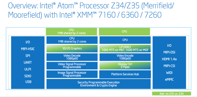
In the first half of the year, Intel will bring out Merrifield - this is the dual-core Silvermont based SoC that's effectively the phone version of Bay Trail. Despite being aimed at the performance and mainstream segments, Intel expects it to be performance competitive with Qualcomm's Snapdragon 800 and Apple's A7. On the modem side, Intel hopes to pair Merrifield with the XMM 7260 LTE modem.

In the back half of the year, Merrifield gives way to Moorefield - this is a quad-core update to the SoC with enhancements to the graphics and display sides. Just as Qualcomm is under pressure to play in the core race, it seems Intel is too.

Cherry Trail is the 14nm update to Bay Trail, featuring Intel's Airmont core (14nm shrink of Silvermont) and a substantial boost in graphics performance (Gen8 graphics, 16 EUs).

The only member of the value segment is Intel's SoFIA. This is an SoC that comes to Intel by way of the Infineon acquisition. The original design featured a low end ARM CPU, but Intel modified it to instead use Intel's Silvermont cores.

It's important to note that Intel's entire mobile roadmap is 64-bit enabled. There are no 32-bit only cores in Intel's mobile future, and Intel's Android development has shifted entirely to a 64-bit focus.

Today the big news is, of course, Merrifield as Intel finally going public about the architecture. It's pretty easy to understand, although this block diagram makes it even easier. The stuff in blue is Merrifield, the solid green is what Moorefield adds and the blue/green is common to both:

Both Merrifield and Moorefield are built on Intel's 22nm SoC process, bringing mobile parity with the rest of Intel's businesses. The parity won't last for long in phones as Intel is expecting to begin its 14nm Broadwell later this year but it's a much better story than it used to be.

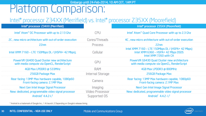
Merrifield features two Silvermont cores sharing a 1MB L2 cache and running at up to 2.13GHz. Moorefield doubles both core count and cache size, while increasing max frequency to 2.3GHz. Intel continues to follow the industry's terrible lead and quotes max turbo frequencies rather than base clocks in its marketing materials.

Intel Merrifield & Moorefield Specs
  Intel Atom Z3460 Intel Atom Z3480 Intel Atom Z3560 Intel Atom Z3580
Codename Merrifield Merrifield Moorefield Moorefield
CPU Cores/Threads 2/2 2/2 4/4 4/4
CPU Max Turbo Clock 1.60GHz 2.13GHz 1.80GHz 2.33GHz
GPU PowerVR G6400 PowerVR G6400 PowerVR G6430 PowerVR G6430
Max GPU Clock 533MHz 533MHz 533MHz 533MHz

Intel continues to embrace the hipocrisy of all mobile SoC vendors and advertises max CPU clocks rather than a true base clock. Just like Bay Trail, Merrifield and Moorefield can share TDP between both the CPU and GPU cores. I have to say that I'm pleased we're dealing with no more than two SKUs per family this time around. I would like to see Intel reduce that to a single one but once Moorefield displaces Merrifield I'll be happy with a two SKU stack.

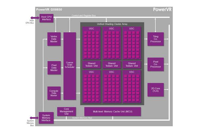
While Intel uses its Gen graphics in Bay Trail, the GPU in both SoCs is still from IMG. Merrifield features the PowerVR Series 6 G6400, while Moorefield uses the G6430. Both are four cluster designs, the latter is just optimized for higher performance. This is roughly the same GPU configuration Apple uses in the iPhone 5s/iPad Air, but at somewhat higher frequencies from what I can tell (and of course, built on Intel's 22nm process and not Samsung's 28nm).

The ISP is all new compared to CloverTrail+. The new ISP tops out at 13MP/2.1MP, which does put it behind the latest from Qualcomm in terms of max supported sensor resolution.

Both SoCs integrate a sensor hub akin to Apple's M7 for use in low power monitoring of sensor data without drawing a lot of power.

Intel isn't talking much about video encode/decode, but it's important to note that there is no hardware accelerated H.265 decode as far as I can tell.

Merrifield presently supports Android 4.4.2 and Intel expects it to support the L-release of Android when it's ready.

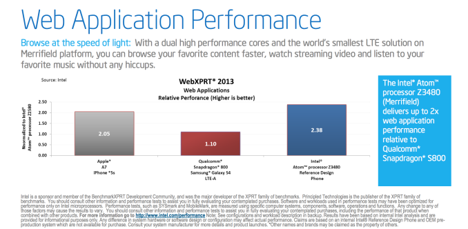
Intel shared a bit of Merrifield performance data, although we weren't able to run any ourselves. Intel's data puts the dual-core Merrifield CPU performance ahead of Apple's 1.3GHz A7 by 16% in WebXPRT. Given how close the Bay Trail/A7 performance race was, Intel's numbers sound believable here.

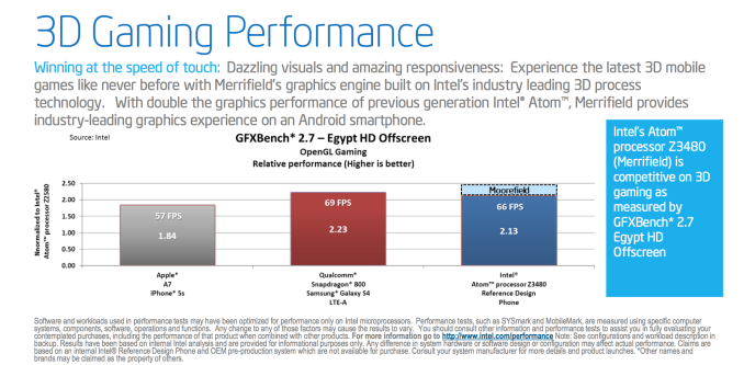
Intel is also claiming a similar GPU performance advantage compared to the A7.

I think it's very telling that Intel no longer seems to have any issue making direct, public comparisons to Apple hardware. It wasn't too long ago that Intel shied away from doing just that. I don't believe this says anything about the Intel/Apple relationship, but perhaps it says something about the intended target for Merrifield. In the past Intel may have hoped to win Apple over, but Merrifield appears to be a design aimed at those who wish to compete with Apple.

As I mentioned earlier, Intel's entire 2014 lineup of mobile SoCs are 64-bit enabled. Intel shared a little bit of data on the peak performance improvement you can expect to see from applications recompiled in x86-64. Google has yet to share its 64-bit Android plans, at this point all 64-bit Android demos are using vendor recompiled kernels and nothing official from Google. I expect this to change at some point this year, it's just a question of when - a question that will likely be answered at this year's Google IO.

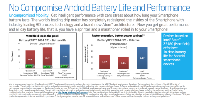
Power is very important when making any performance claims, and Intel is similarly bold with its power efficiency claims. I haven't used BatteryXPRT, but it comes from the same family of mobile benchmarks that Intel loves so dearly. I'll reserve final judgment until we see power data in a broader set of battery tests, but I would hope that at 22nm Intel is able to pull a win here.

Merrifield is an important process and architectural update to Clover Trail+. The move to Silvermont cores puts Intel in a very different performance position, and embracing IMG's PowerVR Series 6 (Rogue) GPU modernizes Intel's GPU story. Intel also has a much better modem story than ever before. For the first time since Intel started its quest to make it into mobile, there's a fairly solid looking modem and AP story. The only thing left is to actually get a meaningful smartphone design win. 

I suspect if Merrifield were available in a good chassis today (Moto X, G2, Nexus 5, etc...) it would make for an excellent device. Intel seems fine with not pursuing absolute performance leadership, but it appears to have built something competitive.

Depending on where Intel prices Merrifield, it could provide quite competitive on the CPU side when pitted against Qualcomm's Snapdragon 610/615. The issue here remains one of design wins, not one of technical proficiency.

ZTE Launches Grand Memo II LTE, Open C at MWC 2014

$
0
0

Grand Memo II LTE

The ZTE Grand Memo II LTE is a phablet that's almost as big as its name with a 6" HD display. ZTE's press kit doesn't actually reference a resolution other than "HD", but it's safe to say that it probably means 720p, as 1080p would be FHD. ZTE is also claiming an 80% display to front face ratio, which would likely be the record for a phone. This is undoubtedly a mid-range phone though, because the SoC is a Snapdragon 400, although there's no clue as to what the SoC actually is. The spec list can be seen below:

  ZTE Grand Memo II LTE
Display 6" 720p IPS LCD
SoC Snapdragon 400
RAM 2 GB
Rear Camera 13MP f/2.2
Front Camera 5MP f/2.2
WiFi 802.11b/g/n/ac
Storage 16GB
Battery 3200 mAh, 3.8V, 12.16 WHr
WCDMA Bands 900/2100 MHz (Band 8, 1)

ZTE is also talking up its new MiFavor 2.3 UI, which actually looks surprisingly well-designed. ZTE isn't saying anything about LTE bands but this definitely will have LTE. The phone has a 7.2mm thickness and a "carbon fiber weave" back, and there's some sort of multiwindow multitasking, along with IR remote functionality. Gorilla Glass 3 is used for the glass lens covering the display. CABC and APT are cited as power saving technologies. CABC would be content-adaptive backlight control which adjusts the backlight while simultaneously brightnening the image to maintain the same image although this can cause visible flickering. ZTE also says that their camera application will allow full manual control of ISO and focus, but it's going to take a device in hand to really know whether this is true. APT would be average power tracking, which would be a way of getting the phone to reduce the amount of power that is consumed by the radio.


ZTE Open C

The ZTE Open C is a 4" Firefox OS phone, one of two new Firefox OS phones that ZTE is launching. There's a 1.2 GHz dual core SoC MSM8210 Snapdragon 200 inside which means Cortex A7, with a 3MP camera, and it would run Firefox OS 1.3. Clearly, this is the phone that comes out of the Mozilla announcement. This is definitely supposed to be a 25USD phone, as there's only WVGA resolution, half a gig of RAM and 4GB internal storage, and 1400 mAh battery. Otherwise, ZTE doesn't seem to be talking up this phone too much.

Broadcom Announces BCM4354 802.11ac 2x2 MIMO Combo for Smartphones

$
0
0

Today Broadcom is announcing the newest member of their popular WiFi/BT/FM series of combo chips, the BCM4354, which adds 2x2 MIMO (two spatial stream) for smartphones and retains 802.11ac capabilities. The BCM4354 includes BT 4.1 / LE support in addition to FM receive, and also incorporates Rezence (the new A4WP) wireless charging receiver functionality. 

By adding a second spatial stream, BCM4354 is capable of a maximum downstream PHY throughput of 867 Mbps with 80 MHz channels, double the single spatial stream 433 Mbps throughput we saw on previous generation flagships. Of course moving to 2x2 MIMO will require an additional antenna for WiFi, or possibly an antenna-sharing architecture with a high band cellular antenna on smartphones that are increasingly packed full of antennas. With the increase in wireless throughput, BCM4354 includes low power PCIe and SDIO 3.0 for WLAN, in addition to UART and USB for bluetooth. 

BCM4354 is already in production and will likely show up in the next crop of smartphones. 

HTC Launches Desire 816 at MWC

$
0
0

Today, HTC seems to be delivering on their promise for a stronger focus on the 150-300 USD market segment by launching the Desire 816, a phablet with a 5.5" 720p display and a Snapdragon 400, along with dual front facing speakers with an amplifier on each speaker. For now, it seems that HTC is quite tight-lipped on software, as they only state that the 816 runs "Android with HTC Sense", although based upon the press images it's clear that the hardware buttons have been removed and it may be the beginning of a trend for HTC's 2014 devices. While many are likely to object over the bezel on the bottom, it seems that this may be an unavoidable bezel, as the One, One max, LG G2, Nexus 5, and other phones all have the glass bezel area around as tall as the one that looks to be on the Desire 816. Based on the photos that I've seen for the HTC One's digitizer, it seems that the area must be used for digitizer connectors, but capacitive buttons will fit in that area.

Of course, specs are effectively the most important part of midrange phones when it comes to placing the kind of value that they have, so I made a table to summarize the key points:

  HTC Desire 816
Display 5.5" 720p LCD
SoC MSM8928, Snapdragon 400, 1.6 GHz quad Cortex A7
RAM 1.5 GB
Rear Camera 13MP f/2.2, 1080p HD recording
Front Camera 5MP f/2.8 720p HD recording
WiFi 802.11 b/g/n
Storage 8GB + microSD
Battery 2600 mAh, 3.8V, 9.88 WHr
WCDMA Bands 850/900/2100 MHz (Band 5, 8, 1)
LTE Bands

EMEA: 800/900/1800/2600 MHz (Band 20, 8, 3, 7)

Asia: 900/1800/2100/2600 MHz (Band 8, 3, 1, 7)

700 MHz (Band 28) for Taiwan, Australia

SIM Size NanoSIM

Overall, outside of pricing, there's not too much to talk about. It does use a NanoSIM, something that's definitely important to keep in mind for prospective buyers, and the 9.88 WHr battery is a bit small for the 5.5" form factor but based upon the performance of the One max with a 5.9" display, it shouldn't be too big of a deal, especially with the power-sipping Cortex A7s. The press release doesn't say anything about the LCD panel, but I guess that will have to be discovered at the press event. Overall though, this seems like a relatively well-designed phablet. Whether HTC's strategy will work is another question.

Gallery: Desire 816

Samsung Announces Galaxy S5: Initial Thoughts

$
0
0

Every year Samsung launches a new Galaxy S flagship smartphone, and as always, Samsung puts the best platform that can be bought in their devices. The Galaxy S5 is no exception, as the MSM8974AC, or Snapdragon 801, powers the Galaxy S5. The 8974AC is the 2.45 GHz bin of the MSM8974AB, a slightly massaged MSM8974 that first launched with the LG G2 and other devices in the summer of 2013. As a recap, the MSM8974AB increases the clock speed of the Hexagon DSP to 465 MHz from 320 MHz, and the LPDDR3 RAM clocks go from 800 MHz to 933 MHz. What really matters though, is that GPU goes from 450 MHz to 578 MHz from 8974 to 8974AC. I definitely have to point to Anand's piece on the Snapdragon 801 for anyone that wants to know more.

The other portion of the hardware story is the camera, which is probably one of the biggest areas for OEMs to distinguish themselves from the pack. Samsung seems to be playing it safe this year with a straight upgrade from 13MP to 16MP by increasing sensor size, and pixel size remains at 1.12 micron side edge length. It is notable that the camera sensor seems to be in a 16:9 aspect ratio, which would make it possible for both photos and videos to keep the same interface without odd reframing effects when going from photo preview to camcorder functionality. Optics are effectively unchanged from the Galaxy S5, as the focal length in 35mm equivalent remains at 31mm, the aperture remains at F/2.2. The one area where there could be a notable improvement is the promised ISOCELL technology, which physically separates pixels better to reduce quantum effects that can lead to lower image resolution and also increases dynamic range, although this will require testing to verify the claims made by Samsung. Samsung has also added 4K video recording for this phone and real time HDR to extend the dynamic range of the camera.

The Galaxy S5 has 2GB of RAM, also not too surprising given the 32-bit ARMv7 architecture of the 8974AC.

The display is a 1080p 5.1” panel, which makes this phone around the same size as the LG G2. Samsung has definitely improved AMOLED, but first impressions are unlikely to tell much when it comes to the quality of calibration and other characteristics of the device. In all likelihood, this will continue to use an RGBG pixel layout in order to improve aging characteristics as the various subpixels age at differing rates. I would expect max brightness to increase, although this may only show in very specific conditions such as extended sunlight exposure and low APL scenarios.

The industrial design seems to be an evolution of the Note 3, with a texture that looks similar to that of the Nexus 7 2012. However, whether the stippled texture will actually avoid the long-term issue of a slimy/oily feel is another question that will have to be answered after the hands-on. While we're still on the point of the hardware design, the Galaxy S5 is IP67 rated, which is why the microUSB 3.0 port has a cover for water and dust resistance.

The fingerprint sensor is a swipe-based one, and Brian has voiced displeasure over swipe sensors like those found in the One max. I personally think that there could be some issues with ergonomics, as Samsung places the home button very close to the edge of the phone, which would make it rather difficult to swipe correctly over the home button, especially if the device is being used with one hand.

As always, Samsung has included removable battery and a microSD slot for those that need such capabilities, although now that Samsung is following Google guidelines regarding read/write permissions, the utility of the microSD slot could be much less than previously expected. For the battery, things are noticeably different as Samsung has gone with a 3.85V chemistry compared to the 3.8V chemistry previously used by the Galaxy S4. With a battery capacity of 10.78 WHr, this means that it has 2800 mAh. For reference, the Galaxy S4 had a 9.88 WHr battery with 2600 mAh. 

As always, Samsung has put TouchWiz on top of their build of Android that will ship with the Galaxy S5, and it mostly looks the same. There are definitely some new features though like My Magazine, which seems to be a way of presenting multiple sources of information using a scrollable list of tiles with images on them.

There might be a trend here in the paragraphs, and while some may see it as a tic, it’s probably more representative of the consistency that Samsung is bringing to the table. “As always” means that people know what to expect, and while it may not be nearly as exciting to the tech press, average people live and die by what’s relatively familiar, not what’s new and exciting. The addition of new features and consistent improvements to performance without compromise relative to the previous generation is definitely something to be applauded, and with review units, hopefully it will be possible to see how the GS5 stacks up against the competition.

At any rate, the phone will launch with blue, black, white, and gold colors. It launches April 11 in 150 countries.


AMD Announces Embedded Radeon E8860 GPU

$
0
0

For the integrated market, there are several levels of capability that manufacturers need to consider.  This is a market driven by sales, thus OEMs that require specific resources are usually catered for.  Thus despite the fact that AMD have an aggressive APU line up on the embedded side (and have the embedded related warranties and support), there is scope for something more powerful.  This is the purpose of the E8860.

The E8860 is a 37W multi-chip-module FCBGA part, with the package measuring 37.5mm x 37.5mm.  The GPU has a PCIe 3.0 interface and implements 640 SPs at 625 MHz.  The GPU uses GCN similar to the HD7000 series, and is paired with 2GB of GDDR5 at 1125 MHz (4.5 GHz effective).  Aside from the usual DX11.1, OpenCL 1.2 and OpenGL 4.2 compatibility we normally see with this GCN, AMD offer a variety of SKUs to cater for the following display output requirements:

AMD E8860 MXM 3.0 (A) + 5 DisplayPort
AMD E8860 PCIe + 2x DVI + mDP
AMD E8860 PCIe + 5x mDP
AMD E8860 PCIe + 4x mDP LPX

Performance is officially listed as achieving P2689 in 3DMark-11 when paired with an AMD R-464L APU.  So the big question here is if the E8860 can be paired with either a BGA or socketed APU in dual graphics mode.  On the consumer side at least, this could result in some nice GPU performance if an APU could be paired with something like this, leaving a PCIe x8 slot for other devices.  It could even act as a mid-range part in the laptop space, although 37W will need to be catered for, or a mini-ITX motherboard where the other PCIe lanes are used for SATA controllers for extra storage.

Due to the use in the embedded market, interested parties will need to contact their local AMD representative for pricing and information.

Source: AMD

LG G Pro 2 and G2 Mini launched: Analysis and Hands-On

$
0
0

LG G Pro 2

At MWC, LG has also announced a few new devices, some that fit in with their previous cadence of releases, and others that are something new. To start with the expected, the successor to the LG G Pro was announced, and it's a worthy successor to the G Pro and a close cousin to the LG G2. It uses a mildly updated version of the Snapdragon 800, the Snapdragon 801 (8974AB), and shares much of the industrial design and material feel with the LG G2, which includes the back-side mounted buttons, the curved back cover, and the same 13MP camera module with OIS for better low light shots.

Of course, there's also plenty that has changed. The display, while still the same 1080p resolution and IPS technology, is now a 5.9" size, which puts it firmly in phablet territory. While it may be large, LG is also claiming a 77.2% screen to frame ratio, which means that it isn't quite as big as a One max in the hand, and more in line with the Note 3. It's also well worth saying that the G Pro 2 has a matted texture that immensely improves in hand feel. The G Pro 2 also continues the G Pro's hardware line with a removable battery and microSD slot, which is why there isn't a curved battery, which is definitely a big reason why the G Pro 2 doesn't have a significantly larger battery than the G2 despite its much larger size, as seen below.

Outside of the hardware upgrades, LG also added some interesting new features. The Knock Code feature basically takes KnockOn and adds the equivalent of a pattern unlock to it, which is a logical next step. LG is emphasizing that this feature will be on all phones launching in 2014, although it's not clear whether this feature would be backported to phones like the LG G2. The Natural Flash feature is also a software feature that uses a photo with the flash off to appropriately set the white balance of the photo taken with a flash. OIS+, another software feature for the camera means EIS (software stabilization) is added on top of the OIS to better filter out unintended motion. While not as effective as increasing the quality of the OIS module due to the need to remove the ghosting image from the sensor, adding EIS will always be more effective than OIS alone.

Also, based on initial use of a demo unit, the G Pro 2 can now have a multitasking button on the navigation bar as seen above, although it's not possible to make the menu key behave as on an AOSP device with software buttons. I really do like the new finish, which has a grippy finish that is miles ahead of the G2 in feel.

The camera is also good, but a lot of the new camera features like the refocus functionality are very much designed for static scenes only, as a shaky hand or any background movement will cause noticeable change in the photo from one level of focus to another, and becomes most obvious when the "all-in-focus" option is selected, which creates ghosting, much like HDR does on fast-moving objects. In a fast and shaky test, it also made for odd results as the first photo was less detailed (due to blur) than the next closer focal point. This is effectively a fact of life when it comes to any phone that doesn't do this functionality in hardware with a Lytro-style camera, so the Galaxy S5 will also have this issue. I also thought that such a function would have more gradations to levels of focus to allow for fine-tuning out of focus photos, but there's only around four different levels of focus between infinity and the minimum possible.

LG also continues to include the manual focus slider for situations where auto-focus fails, which should be included by more OEMs.

One of the most immediate things I also noticed was that LG continues to fill half of the notification space with things like QSlide, quick settings, and other various extra items. I question the wisdom of doing so, but as far as I recall, most of the unnecessary items can be hidden to restore some level of sanity. 

LG G2 Mini

LG also announced the G2 mini, a smaller version of the LG G2. While it's similar, it's more in the same vein of the G Pro 2 when it comes to the overall material feel, which is an evolution of the LG G2, so the shape is largely the same, although there's no word on whether it retains the curved battery. The hardware spec is definitely not at the same level at the G2, but it's tough to say whether the value proposition is gone. The SoC goes from the Snapdragon 800 to Snapdragon 400, or Tegra 4i. This would mean either a quad core Cortex A7 for all but Latin America, which gets the Tegra 4i which has a quad core Cortex A9r4 at 1.7 GHz. Both versions have LTE, which means it's the MDM9x25 block in the Snapdragon version as a part of MSM8926, and Icera i500 in the Tegra 4i part. Unfortunately, the only demo units available were the MSM8x26 parts, as seen below.

Outside of the SoC, the camera goes down to 8MP, but it's unsure whether the sensor is 1/3" or 1/4". The display is definitely smaller at 4.7" with a qHD panel, which would mean the resolution is below both the GS4 Mini and the One Mini.

Nokia launches the X, X+, and XL at MWC

$
0
0

Nokia X

Nokia has finally launched the long-rumored Nokia X running Android, and it's well worth going over Nokia's first Android phones. The first phone is the Nokia X, which is an MSM8225-platform device, with a dual core 1 GHz Cortex A5 inside and Adreno 203 GPU. There's 4GB of internal storage and 512 MB of RAM. The display is a WVGA IPS panel at 4" in size, and there's a 1500 mAh, 3.7V battery inside of the phone. The camera is a 3MP, fixed focus unit with a 1/5" sensor size and F/2.8 aperture, and video recording is limited to FWVGA. Needless to say, this is a budget device, and at 89 EUR or so, it could be an interesting device.

On the software side, the Nokia X runs Android 4.1.2 with Nokia's skin on top that makes it look like Windows Phone.

Nokia X+

The Nokia X+ is effectively identical to the Nokia X, the sole difference that I have seen is that the X+ has 768MB of RAM, and will go on sale for 99 EUR.

Nokia XL

The Nokia XL is slightly different from either the X or the X+. Battery capacity goes up to 2000 mAh, the camera is upgraded to a 5MP module with 1/4" sensor and adjustable (auto) focus. The display is also made to 5", but it remains the same WVGA resolution with IPS display technology. It will cost 109 EUR.

All of these phones also have Dual SIM capabilities, and will have Nokia's suite of applications at launch.

Nokia X Development

In the Nokia Developer Keynote today, the platform for Nokia X was explained at a high level in order to answer a number of questions that were asked since the recent announcement.  Simply put, the extra Nokia layer over the base modifiable Android system should not interfere with Android mobile development.  App developers will have to submit their apps to the Nokia X store, but Nokia expects 99% of all apps to work straight away.  A system is set up such that any developer APK can be checked online in a few minutes – upload and get an answer if it will work.  Nokia Store validation will take a little longer when the app is submitted (Lunagames stated that Highway Hei$t took a day). Also of note was the discussion regarding strategy.

 Due to Nokia X positioning itself in emerging markets as a user’s first/second smartphone, and in regions where users might not have access to credit cards, the focus is on carrier billing.  Nokia are providing a module for APK development to help enable this.

MWC 2014: Wilocity brings WiGig 802.11ad to Smartphones with Wil6300 Chipset

$
0
0

News just dropped through from Wilocity about its new Wil6300 chipset announced at Mobile World Congress.  The Wil6300 chipset is quoted as the world’s first 802.11ad ‘WiGig’ multi-gigabit WiFi chipset for smartphones.  Wilocity are stating a peak speed of 4.6 Gbps over an 802.11ad network, equivalent to 8-antenna based WiFi.  So while 802.11ad can have limited range (10m with no walls) due to the 60 GHz frequency band used, there is scope in home and work user environments for faster in-network data streaming, such as video. 

Wilocity has a history of WiGig development – we covered their desktop PC 802.11ad development back at Computex 2012 and sales figures for Wilocity number more than a million since February 2013.  In the mobile space, this new chipset is built on a 28nm process and power use is expected in the 200-300mW range in use.  While idle, power consumption is rated at sub 1mW, and the 700mW total power quoted above is for pure file transfer.

I had a chance to pop by the Wilocity booth at MWC2014.  Its 802.11ad demo was working with devices from their partners, namely a Dell tablet streaming to a box with 2K content and showing file transfer between two 802.11ad enabled tablets:

For the mobile phone demonstration, a Samsung phone was retrofitted with Wilocity's 2014 Falcon platform and peak statistics of were being shown:

Wilocity’s development cycle puts mobile based 802.11ad in the 2015 space.  They are working with ‘the usual players’ in the market.  The module we were shown implemented 802.11n and 802.11ad in the same device, and I was quoted that with economies of scale the price of the 802.11ad module could be brought down to that of 802.11ac.  Wilocity is also using beamforming to help improve quality at extended ranges, with up to 50 meters being tested and confirmed, albeit at lower speeds.  The main issue is walls, which they are working on.


Western Digital Targets Surveillance Storage Market with Purple Hard Drives

$
0
0

Western Digital's campaign to delineate hard drive market segments and the accompanied colour-based branding has proved to be very popular. The Red drive lineup for the SMB / SOHO NAS market and the Black drives for the enthusiast segment have been greeted with good market acceptance. Today, Western Digital is expanding this initiative with the Purple branding for hard drives targeting the growing surveillance market (NVRs and NAS units dedicated to recording feeds from IP cameras).

Background

All SATA hard drives fulfill the same basic functionality of storing data on platters. Most hard drives use the same hardware circuitry (except for enterprise drives which have features such as RAFF - Rotary Accelerated Feed Forward - that require extra sensors on the drive to better handle vibrations in storage arrays). The scope for differentiation boils down to the firmware. The SATA protocol has a number of optional features intended to improve performance for specific scenarios. One example is NCQ (Native Command Queuing), which allows for reordering of commands to improve efficiency. Another example is the ATA Streaming Command Set, which targets A/V setups by providing features targeting video payloads. Drives targeting the A/V and surveillance markets can optimize the firmware around this optional specification.

History

Western Digital has been serving the DVR / STB / surveillance storage market with the WD-AV GP product line for quite some time now. Hardware-wise, these drives happen to be the same as the Green drives, but the difference happens to be in the firmware. WD's ATA Streaming Command Set implementation under the SilkStream tag supports up to 12 simultaneous HD streams.

Most NVRs are based off NAS platforms in RAIDed environments. Since the WD-AV-GP drives were not specifically geared for use in NAS devices, it makes sense for WD to develop firmware optimized for video surveillance storage using the Red drives as the hardware base. The result is the WD Purple lineup.

Features and Specifications

The Purple hard drives (WDxxPURX) are dedicated to service the surveillance market. Similar to the WD-AV GP lineup, these are also built for 24x7 operation. The SilkStream tag for the optimized firmware in the WD-AV GP lineup is replaced by AllFrame in the WD Purple. The optimizations work with the ATA Streaming Command Set to improve playback performance and reduce errors / frame loss. While SilkStream was advertised to support up to 12 simultaneous HD streams, AllFrame is designed to support up to 32 HD cameras / channels. Obviously, advantage of the AllFrame technology is possible only with the host controller support. It goes without saying that the appliance vendor must be in the compatibility list provided by WD in order to take advantage of the surveillance-specific features in the Purple drives.

Similar to the Red drives, these come with the IntelliPower feature (rotational speed of 5400 rpm) and TLER enabled. IntelliPower enables WD to provide best-in-class power consumption numbers with the Purple drives. There is no RAFF support on-board, though, as these are meant for table-top appliances with 1 to 8-bays. The drives are rated for workloads up to 60 TB/yr. For reference, recording 4 x 1080p30 streams for 365 days requires 200 TB of storage. SD streams come with lower storage cost. In any case, putting the WD Purples in RAID with multiple drives should easily keep workloads for each drive under 60 TB/yr. For SMB / SME surveillance setups requiring up to 64 cameras, WD suggests the use of Se drives, while mission-critical applications are advised to utilize the more powerful Re drives.

The 3.5" Purple drives come in 1, 2, 3 and 4 TB capacities. WD has a number of launch partners including, but not limited to, PELCO, HikVision, Synology and QNAP.

In other news, Seagate also announced the Surveillance HDD yesterday, targeting the surveillance market. Unfortunately, we weren't briefed extensively about it, but the specs seem similar to that of the Purple lineup (except for the addition of RV - rotational vibration - sensors for operating in multi-drive environments, which seems similar to RAFF technology).


Viewing all 3357 articles
Browse latest View live