Quantcast
Channel: AnandTech Pipeline
Viewing all 3357 articles
Browse latest View live

Intel Reveals New Haswell Details at ISSCC 2014

$
0
0

As of late, Intel has been unusually guarded about releasing information about its microprocessor designs. Haswell launched last year with great architecture disclosure, but very limited disclosure about die sizes, transistor counts and almost anything surrounding the interface between Haswell and its optional embedded DRAM (Crystalwell) counterpart. This week at ISSCC, Intel will finally be filling in some of the blanks. 

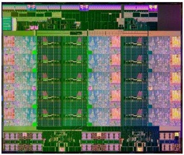
The first bit of new information we have are official transistor counts for the range of Haswell designs. At launch Intel only disclosed transistor counts and die areas for Haswell ULT GT3 (dual-core, on-die PCH, GT3 graphics) and Haswell GT2 (quad-core, no on-die PCH, GT2 graphics). Today we have both the minimum and maximum configurations for Haswell. Note all transistor counts below are schematic not layout:

Intel Haswell
  CPU Configuration GPU Configuration Die Size Transistor Count
4+3 Quad-Core GT3e 260mm2 + 77mm2 1.7B + ?
ULT 2+3 Dual-Core GT3 181mm2 1.3B
ULT 2+2 Dual-Core GT2 (est) ~180mm2 (est) ~1B
4+2 Quad-Core GT2 177mm2 1.4B
2+2 Dual-Core GT2 130mm2 0.96B

I've organized the table above by decreasing die size. I still don't have confirmation for the ULT 2+2 configuration, but the rest is now filled in and accurate. If you remember back to our Iris Pro review, I measured the die area for Haswell GT3 and the Crystalwell eDRAM using some cheap calipers. I came up with 264mm2 + 84mm2, the actual numbers are pretty close at 260mm2 + 77mm2.

Doing some rough math we see that the addition of a third graphics slice to a Haswell core accounts for around 300M transistors. That would put the ULT2+2 configuration at around 1B total transistors. I suspect the ULT 2+2 configuration is similar in size to the quad-core + GT2 configuration.

Next up on the list is some additional information on the Crystalwell (embedded DRAM) design and configuration. Intel explained how it arrived at the 128MB L4 eDRAM cache size, but it wouldn't tell us the operating frequency of the memory or the interface between it and the main CPU die. In its ISSCC disclosures, Intel filled in the blanks:

The 128MB eDRAM is divided among eight 16MB macros. The eDRAM operates at 1.6GHz and connects to the outside world via a 4 x 16-bit wide on-package IO (OPIO) interface capable of up to 6.4GT/s. The OPIO is highly scalable and very area/power efficient. The Haswell ULT variants use Intel's on-package IO to connect the CPU/GPU island to an on-package PCH. In this configuration the OPIO delivers 4GB/s of bandwidth at 1pJ/bit. When used as an interface to Crystalwell, the interface delivers up to 102GB/s at 1.22pJ/bit. That amounts to a little under 1.07W of power consumed to transmit/receive data at 102GB/s.

By keeping the eDRAM (or PCH) very close to the CPU island (1.5mm), Intel can make the OPIO extremely simple.

Intel also shared some data on how it achieved substantial power savings with Haswell, including using a new stacked power gate for the memory interface that reduced leakage by 100x over Ivy Bridge. Haswell's FIVR (Full Integrated Voltage Regulator) is also a topic of discussion in Intel's ISSCC papers. FIVR ends up being 90% efficient under load and can enter/exit sleep in 0.32µs, requiring only 0.1µs to ramp up to turbo frequencies.

Intel's Haswell ISSCC disclosures don't really change anything about Haswell, but they do further illustrate just how impressive of a design it is.


AMD Announces Radeon R7 250X; Shipping Today

$
0
0

As it turns out, February is going to be a busy month for GPUs. Normally February is something of a quiet month, surrounded by CES on one side and GPU trade shows like NVIDIA’s GTC on the other, but for 2014 we’ve seen and will continue to see a number of important launches as the month rolls on. The start of this month saw the launch of AMD’s first Mantle enabled drivers and the first Mantle enabled software, and today AMD is back with a new and somewhat low-key product launch to help fill out their product stack.

Launching today is AMD’s new anchor for the $99 price point, the Radeon R7 250X. The 250X is intended to fill a price and performance gap between the low-end Oland based R7 250, and the more powerful but more expensive R7 260 series. This anchor position was previously filled by the 250 at $89, but due to a combination of slow uptake on the R7 260 and competitive pressure, AMD has decided to push out something more powerful at $99.

Since the R7 250 was already a fully enabled Oland part, and the R7 260 was already a cut-down Bonaire part, to fill the gap AMD is calling their GCN 1.0 based Cape Verde GPU back into service. Cape Verde powered what’s now the officially discontinued Radeon HD 7700 series, spending most of its life serving as AMD’s sub-$150 budget backbone. For 250X AMD is going to be doing a straight rebadge of the most powerful 7700 part, the 7770 GHz Edition, bringing the 7770 into the Radeon 200 family. This is similar to what AMD did a couple of years back with the 5700 series, ultimately rebadging the entire series as the 6700 series. We're not fans of the practice, but with the 200 series already containing a mix of old and new GPUs, this is hardly disruptive.

AMD GPU Specification Comparison
  AMD Radeon R7 260X AMD Radeon R7 260 AMD Radeon R7 250X AMD Radeon R7 250
Stream Processors 896 768 640 384
Texture Units 56 48 40 24
ROPs 16 16 16 8
Core Clock ? ? 1000MHz 1000MHz
Boost Clock 1100MHz 1000MHz N/A 1050MHz
Memory Clock 6.5GHz GDDR5 6GHz GDDR5 4.5GHz GDDR5 4.6GHz GDDR5
Memory Bus Width 128-bit 128-bit 128-bit 128-bit
VRAM 2GB 1GB 1GB/2GB 1GB
FP64 1/16 1/16 1/16 1/16
TrueAudio Y Y N N
Transistor Count 2.08B 2.08B 1.5B N/A
Typical Board Power 115W 95W 95W 65W
Manufacturing Process TSMC 28nm TSMC 28nm TSMC 28nm TSMC 28nm
Architecture GCN 1.1 GCN 1.1 GCN 1.0 GCN 1.0
GPU Bonaire Bonaire Cape Verde Oland
Launch Date 10/11/13 01/14/14 02/10/14 10/11/13
Launch Price $139 $109 $99 $89

Since the 250X is a straight 7770 GHz Edition rebadge, we won’t spend too much time going over the specifications since we’ve reviewed this before. With 640 SPs and 16 ROPs, it sits comfortably between the more expensive 260 series and the existing Oland based R7 250 in specifications and performance. Both Oland and Cape Verde are GCN 1.0 GPUs, so while the fact that both GPUs share the 250 series name is a minor annoyance, from a feature standpoint they’re going to be identical. Though this does mean that the 250X will be at a feature disadvantage relative to the GCN1.1 based 260 series, lacking TrueAudio support among other features, giving buyers a tangible reason to step up to the 260 series.

GPU specifications aside, let’s quickly talk about memory. This launch is being done on a very short turn around, so we haven’t been able to get AMD to confirm the complete memory specifications for the 250X. Historically, sub-$100 AMD cards almost always feature a mix of GDDR5 and DDR3, and it’s unclear at this moment whether the same will be happening for the 250X. AMD has told us that there will be 1GB and 2GB cards, which leads us to believe that we’re going to be seeing 1GB GDDR5 cards and 2GB DDR3 cards side-by-side, especially if AMD’s partners want to offer 2GB cards at $99. The specifications we’re going with for now are AMD’s official specifications, which cite GDDR5, but we’ll update this once we get confirmation. DDR3 would significantly cripple the performance of the 250X, so if this comes to pass the GDDR5 version of the 250X would be the only one worth serious consideration.

Meanwhile from a performance perspective the 250X is going to be quite a bit more powerful than the 250 for a very minor price increase. The big increase in stream processors and ROPs directly translates into a big increase in performance, with the 250X set to outperform the 250 by 30-50%. From a practical perspective this means that while the 250 struggled with 1080p at any quality setting, the 250X should be comfortably above 30fps in most games at low settings. Next to the slightly higher price tag, the only real tradeoff for the 250X will be power consumption; 250 remains as AMD’s best sub-75W card, while 250X will require 95W and an external PCie power connector, just as 7770 before it.

Since the 250X is a 7770 rebadge and there isn’t any “new” performance data to look at, we’ll skip an in-depth look at performance. For $99 it should generally outperform anything else for the price, as we can see below in Bioshock Infinite.

Bioshock Infinite - 1920x1080 - High Quality

Our full benchmarks for the 250X/7770 can be found on our GPU Bench 2014 page.

AMD tells us that 250X should be shipping today, though given the fact that we’re in the middle of the Chinese New Year we’re taking a wait-and-see attitude on that. But because it’s a rebadge 250X will take relatively little work to start production on; for AMD’s partners there is little to do besides resuming 7770 production with an updated BIOS and new branding. So we expect that most 250X cards will be identical to their 7770 predecessors, with modifications made as necessary to support the 2GB configuration.

Finally, at $99 the 250X will be launching into a very dense cluster of competitors. Against AMD’s other sub-$100 cards it should perform favorably, significantly outperforming both the R7 250 and 7750, the latter of which continues to be readily available around $99 despite being formally discontinued months ago. The R7 260 series on the other hand should outperform the 250X, but with the 260 minimally available due to low uptake and well off its $109 MSRP as a result, the only meaningful competitors for the 250X are the 260X and the 250, securing the 250X’s place. As an added bonus, this means that the 250X will be launching at a lower price than the original 7770 is currently available at (~$110), making the 250X a de-facto price cut for the 7770.

As for the NVIDIA competition, the closest competitor to the 250X is currently the GTX 650, which has an average price a bit over $100. 650 never did fare well against the 7770, so the 250X should easily enjoy a 20%+ performance advantage. 650 Ti will be much closer in performance, but outside of the occasional sale is almost always found at $120 or more.

Winter 2014 GPU Pricing Comparison
AMD Price NVIDIA
Radeon R9 270X $250  
Radeon R9 270 $210  
  $190 GeForce GTX 660
Radeon R7 260X $140  
Radeon R7 260 $125 GeForce GTX 650 Ti
Radeon R7 250X $100 GeForce GTX 650
Radeon R7 250 $90 GeForce GT 640


ARM Cortex A17: An Evolved Cortex A12 for the Mainstream in 2015

$
0
0

ARM has been doing a good job figuring out its PR strategy as of late. In the span of a couple of years we went from very little outward communication to semi-deep-dives on architecture and a regular cadence of IP disclosures. ARM continues its new trend today with the announcement of its 2015 mid-range CPU IP: the Cortex A17.

As its name implies, the Cortex A17 is a 32-bit ARMv7-A CPU design (64-bit ARMv8 cores belong to the Cortex A50 series - e.g. A53/A57). The best way to think about Cortex A17 is as an evolution of the recently announced Cortex A12, rather than anything to do with the Cortex A15. ARM's Cortex A17 takes the basic 2-wide out-of-order architecture of the Cortex A12 and improves it. Specific details are still light at this point, but I'm told that the front end and execution engine are similar to Cortex A12, with most of the performance/efficiency gains coming from improvements to the memory subsystem. 

The result is a design that is roughly 60% faster than a Cortex A9r4 at a given frequency/process/memory interface (Cortex A12 is 40% faster than A9r4 under the same conditions). Using ARM's own DMIPS/MHz ratings I threw together a little table of relative/estimated performance ratings to help put all of this in perspective:

ARM 2014/2015 CPU IP lineup
CPU IP Target Estimated DMIPS/MHz big.LITTLE Shipping in Devices/Systems
Cortex A57 High-end mobile/servers 5* Yes (w/ A53) 2015
Cortex A53 Low-end mobile 2.3 Yes, LITTLE, w/ A57 2H 2014
Cortex A17 Mid-range mobile 4.0* Yes, big, w/ A7 Early 2015
Cortex A15 High-end mobile 4.0* Yes, big, w/ A7 Now
Cortex A12 Mid-range mobile 3.5 No 2H 2014
Cortex A9 High-end mobile 2.5 No Now
Cortex A7 Low-end mobile 1.9 Yes, LITTLE, w/ A15/A17 Now

*Estimate based on ARM's claims

On a given process node, the Cortex A17 can occupy around 20% more area than a Cortex A9 or a marginal increase over a Cortex A12 design. Running the same workload, ARM expects the Cortex A17 to be 20% more energy efficient than the Cortex A9 (race to sleep), but I'd expect higher peak power consumption from the A17. The Cortex A17 name was deliberately chosen as ARM expects to be able to deliver similar performance to the Cortex A15 (in mobile apps/benchmarks, likely not in absolute performance), but in a much smaller area and at a lower power. I can't help but wonder if this is what the Cortex A15 should have been from the very beginning, at least for mobile applications.

ARM expects many early Cortex A17 designs to be built on a 28nm process, with an eventual shift over to 20nm once the cost of that process drops. ARM supplied an interesting slide showcasing the number of transistors $1 will buy you as a function of process node:

If you're a fabless semiconductor, it looks like 28nm will be the sweet spot for manufacturing for a little while.

Keep in mind that the target market for the Cortex A17, like the Cortex A12, is somewhere in between a device like the Moto G and the latest flagship Galaxy S device from Samsung. 

big.LITTLE Support

If you remember back to our analysis of the Cortex A12, the first version of the core didn't support ARM's big.LITTLE (lacking the requisite coherent interface) but a future version was promised with big.LITTLE support. The Cortex A17 is that future version. In a big.LITTLE configuration, the Cortex A17 will function as the "big" core(s) while the Cortex A7 will serve as the "LITTLE" core(s).

Rather than giving the Cortex A12 a new major revision number, ARM improved the design, added big.LITTLE support and called the finished product the Cortex A17. It's an interesting approach to dealing with the fact that ARM can rev/improve a single IP offering many times over the course of its life. In case it isn't already obvious, there won't be a big.LITTLE version of the Cortex A12.

ARM expects some overlap between Cortex A17 and Cortex A12. If a customer is looking to ship in 2014, Cortex A12 will be the only option for them in the mid-range from ARM. If a customer wants big.LITTLE or they are starting a design now, Cortex A17 is the obvious fit. I expect Cortex A17 will contribute to a relatively short lifespan for Cortex A12 in the grand scheme of things.

ARM sees some of the biggest opportunities in addressing the entry level and performance mainstream smartphone markets going forward. With the Cortex A17 aiming at the latter, ARM sees a potential market of around 450 million devices in 2015. The lack of 64-bit support makes ARM's mid-range lineup a little odd, especially considering the Cortex A53 and Cortex A57 will ensure both entry level and high-end smartphones will be 64-bit enabled. While I don't have an issue with a good mid-range device shipping without 64-bit support, I'm not sure how handset and tablet OEMs will feel. With Apple, Intel (and likely Qualcomm), embracing 64-bit-only strategies in mobile, I do wonder just how much success these A12/A17 architectures will have over the long run.

ARM tells me we should see the first devices using Cortex A17 CPU cores shipping in early 2015. Cortex A17 IP will be available to ARM customers for implementation by the end of this quarter.

Intel Readying 15-core Xeon E7 v2

$
0
0

Reports from ISSCC are coming out that Intel is preparing to launch a 15-core Xeon CPU.  The 15-core model was postulated before Ivy Bridge-E launch, along with 12-core and 10-core models – the latter two are currently on the market but Intel was rather silent on the 15-core SKU, presumably because it harder to manufacturer one with the right voltage characteristics.  Releasing a 15-core SKU is a little odd, and one would assume is most likely a 16-core model with one of the cores disabled – based on Intel’s history I doubt this core will be able to be re-enabled should the silicon still work. I just received the official documents and the 15 core SKU is natively 15-core.

Information from the original source on the top end CPU is as follows:

  •  4.31 billion transistors
  •  Will be in the Xeon E7 line-up, suited for 4P/8P systems (8 * 15 * 2 = 240 threads potential)
  •  2.8 GHz Turbo Frequency (though the design will scale to 3.8 GHz)
  •  150W TDP
  •  40 PCIe lanes

Judging by the available information, it would seem that Intel are preparing a stack of ‘Ivytown’ processors along this design, and thus a range of Xeon E7 processors, from 1.4 GHz to 3.8 GHz, drawing between 40W and 150W, similar to the Xeon E5 v2 range.

Predictions have Ivytown to be announced next week, with these details being part of the ISSCC conference talks.  In comparison to some of the other Xeon CPUs available, as well as the last generation:

Intel Xeon Comparison
  Xeon E3-1280 v3 Xeon E5-2687W Xeon E5-2697 v2 Xeon E7-8870 Xeon E7-8890 v2
Socket LGA1150 LGA2011 LGA2011 LGA1567 LGA2011
Architecture Haswell Sandy Bridge-EP Ivy Bridge-EP Westmere-EX Ivy Bridge-EX
Codename Denlow Romley Romley Boxboro Brickland
Cores / Threads 4 / 8 8 / 16 12 / 24 10 / 20 15 / 30
CPU Speed 3.6 GHz 3.1 GHz 2.7 GHz 2.4 GHz 2.8 GHz
CPU Turbo 4.0 GHz 3.8 GHz 3.5 GHz 2.8 GHz 2.8 GHz
L3 Cache 8 MB 20 MB 30 MB 30 MB 37.5 MB
TDP 82 W 150 W 130 W 130 W 155 W
Memory DDR3-1600 DDR3-1600 DDR3-1866 DDR3-1600 DDR3-1600
DIMMs per Channel 2 2 2 2 3 ?
Price at Intro $612 $1885 $2614 $4616 >$5000 ?

According to CPU-World, there are 8 members of the Xeon E7-8xxx v2 range planned, from 6 to 15 cores and 105W to 155W, along with some E7-4xxx v2 also featuring 15 core models, with 2.8 GHz being the top 15-core model speed at 155W. 

All this is tentative until Intel makes a formal announcement, but there is clearly room at the high end.  The tradeoff is always between core density and frequency, with the higher frequency models having lower core counts in order to offset power usage.  If we get more information from ISSCC we will let you know.

Original Source: PCWorld

Update: Now I have time to study the document supplied by Intel for ISSCC, we can confirm the 15-core model with 37.5 MB L3 cache, using 22nm Hi-K metal-gate tri-gate 22nm CMOS with 9 metal layers.  All the Ivytown processors will be harvested from a single die:

Ivytown Die Shot

The design itself is capable of 40W to 150W, with 1.4 GHz to 3.8 GHz speeds capable.  The L3 cache has 15x 2.5MB slices, and data arrays use 0.108µmcells with in-line double-error-correction and triple-error-detection (DECTED) with variable latency.  The CPU uses three clock domains as well as five voltage domains:

Level shifters are placed between the voltage domains, and the design uses lower-leakage transistors in non-timing-critical paths, acheving 63% use in the cors and 90% in non-core area.  Overall, leakage is ~22% of the total power.

The CPUs are indeed LGA2011 (the shift from Westmere-EX, skipping over Sandy Bridge, should make it seem more plausible), and come in a 52.5x51.0mm package with four DDR3 channels.  That would make the package 2677 mm2, similar to known Ivy Bridge-E Xeon CPUs.

CPU-World's list of Xeon E7 v2 processors come from, inter alia, this non-Intel document, listing the 105W+ models.

I'M Intelligent Memory to release 16GB Unregistered DDR3 Modules

$
0
0

After talking about Avoton and Bay Trail on Twitter, I was approached by the company heading up the marketing and PR for I’M Intelligent Memory regarding a few new products in the pipeline different to what we had seen in the market previously.  The big one in my book is that they are currently sampling 16GB unregistered DDR3 modules ready for ramping up production.

Currently in the consumer space we have 8GB unregistered modules, usually paired together for a 16GB kit.  These use sixteen 4 Gb memory packages on board to total up to the 8 GB number, and are packaged in speeds up to 2933+ MT/s.  Intelligent Memory are a company (or series of smaller individual companies) that have new IP in the market to tie two of these 4 Gb dies together into a 8 Gb die, and are thus able to double the capacity of memory available in the market.

I have been speaking with Thorsten Wronski, President of Sales and Technology at Memphis AG, the company heading up the business end of the Intelligent Memory plan.  We went into detail regarding how the new IP works (as much as I could be told without breaking NDA):

DRAM stacking is unlike NAND stacking.  We have seen manufacturers stick 16 NAND dies onto a single package, but DRAM requires precise (picosecond level) timing to allow the two 4 Gb dies to act as a single 8 Gb package.  This is the new IP to the table, which can apply to both unregistered and registered memory, as well as ECC memory.

The JEDEC specifications for DDR3 do account for the use of 8 Gbit packages (either one 8 Gbit die or two 4 Gbit dies per package), should these be available.  However I am told that currently there is a fundamental non-fixable issue on all Intel processors (except Avoton and Rangeley, other Silvermont (BayTrail) is affected) that means that these dies are not recognised.  In their specifications for Ivy Bridge-E, Intel do state that 8Gb packages are supported (link, page 10), however this apparently has not been the case so far and I'M is working with motherboard manufacturers to further pin down this issue.

Typically the access of a memory chip requires a column and a row, both of which are multiplexed across a set of 16 connects.  With a 4 Gbit package, to access the row, all 16 are used (A0 to A15), whereas a column uses 10 (A0 to A9).  In the 8 Gbit package, the column also requires A11, all part of the JEDEC spec.  This works on Avoton/Rangeley, but not on any other Intel processor, according to Intelligent Memory, and the exact nature of the issue is down to Intel’s implementation of the specification.  I suspect that Intel did not predict 8 Gbit packages coming to market at this time, and have found an efficiency improvement somewhere along the line.  Perhaps needless to say, Intel should be supporting the larger dies going forward.

The dies that I’M are using are 30nm, and according to them the reason why Hynix/Samsung et al have not released an 8 Gbit DRAM die up until this point is that they are waiting until 25nm in order to do so – this is why I’M is very excited about their product.  It could also mean that users wanting HSA implementations under Kaveri could have access to 64GB of DRAM to play with.  But it also means that when 8 Gbit 25nm DRAM dies become available, I’M will perhaps try for a 16 Gbit package for 32GB modules - all aimed for DDR4 I would imagine.

I’M Intelligent Memory is currently a couple of weeks out from sampling our server guru Johan with some of these modules, so hopefully we will get an insight from him as to how they are looking.  They are intending to go down two routes with their product – selling the combined die packages and selling modules.  I have been told that one of the normal end-user manufacturers has already expressed interest in the packages (rated at DDR3-1600), which they would place onto their own DRAM sticks and perhaps bin the ICs for higher speed.  The modules will be sold also via a third-party that often deals in bulk sales.

Mass production is set to begin in March and April, with initial pricing per 16GB module in the $320-$350 range for both DIMM and SO-DIMM, ECC being on the higher end of that range.  To put that into perspective, most DRAM modules on sale today for end-users are in the $8-$14/GB range, making the modules have a small premium which is understandable to get the higher density. 

If this IP holds up to the standard, I would not be surprised if it is purchased (or at the very least observed) by the big DRAM manufacturers.  I expect these modules will first see the light of day in servers (Avoton based most likely), and I will keep an eye out if any end-user manufacturers get a hold of some.  I’M have verified the modules on AMD FX processors (FX-6300 and FX-8320 on 990FX/AM3+) as well as AMD's 760G and A75 (FM2 socket) chipsets.  I was forwarded the following screenshot of two of these modules in an MSI FM2-A75MA-P33 motherboard, which is a dual DRAM module motherboard using the FM2 socket for Trinity APUs:

Here each of the 16GB modules (shown in the SPD tab of CPU-Z) are running at DDR3-1600 11-11-11, giving the two DRAM slot motherboard a total of 32GB of addressable space.

Aside from unregistered modules, I’M are also planning ECC UDIMM and RDIMM versions as well, such as 16GB very-low-profile RDIMMs and 16GB ECC SO-DIMMs.  Non ECC SO-DIMMs are also being planned.  A lot of their focus will be the supply of DRAM components for the direct integration onto automated systems where memory counts are fixed, for systems that use Marvell, TI, Freescale, Xilinx, Altera, Renesas and so on.

AMD’s DockPort Given Virtual Overview

$
0
0

Flying somewhat under the radar, DockPort from AMD is designed to be a low-cost all-in-one solution for external connectivity for a PC or tablet.  Sound familiar?  Like Thunderbolt familiar? This is AMD’s solution to the issue of connectivity, using the DisplayPort connector to transfer USB information as well as audio/visual.

Not a lot has been said about DockPort, despite originally being given a name sometime in 2012, but since CES 2014 has been adopted as an official DisplayPort standard extension by VESA with a finalized standard expected in Q2.  With the combination of DisplayPort and USB 3.0 over a single cable, AMD’s video explains it best how it can be used:

To list the possible uses:

  • Charging (over USB 3.0 standard we would assume)
  • Docking to an external keyboard/battery/audio
  • Connecting Storage, Audio outputs, Video outputs, USB hubs
  • Share video or run multiple video screens

Basically this is everything USB can do, including video stream via DisplayPort, albeit in a single interface that is already standard across many systems and form factors.  AMD have not specified what extra hardware is needed beyond DisplayPort compatibility (presumably the next iteration of the DisplayPort standard) or whether this extension is just for limited use with a bridge chip.  DockPort verified cables will be needed, and no idea on the cost of those this early in the development cycle, or whether the standard will be roped into DisplayPort fundamentally.  The main competition is of course with Intel's Thunderbolt, where one of the features I am most looking forward to is Graphics over TB.  That will not be possible with DockPort, but it will try to do everything else it seems, although it does seem to suggest that DockPort will be limited to USB 3.0 for any data-related daisy chaining, unless AMD have an ace up their sleeve.

I would imagine AMD would tie this technology into their desktop motherboard line, as well as their SoCs, when it is ready which might increase adoption rates faster than Thunderbolt.  Having both interfaces use a similar sort of connector asks the question whether the two interfaces might be coherent in the same output/input, making future devices (namely storage) able to use both in one connector rather than have specific DockPort/TB inputs.

This is still early days, given the computer generated nature of AMD’s video.  Computex is still several months away – we might see an real world update then.  Looking forward to it…!


Radeon R9 290X Retail Prices Hit $900

$
0
0

Though we keep track of video card pricing regularly on an internal basis, it’s not something we normally publish outside of our semi-regular buyer’s guides. More often than not video card pricing is slow to move (if it moves at all), as big price shifts come in concert with either scheduled price cuts or new product introductions. But in a process that has defied our expectations for more than a month now, even we can’t fail to notice what Radeon prices are quite literally up to.

In a sign of the daffy times we live in, Radeon R9 290X prices have hit $900 this week at Newegg. Every card, from the reference models to the water block model, is now at $899, with Newegg apparently doing brisk enough business to be sold out of more than half of their different 290X SKUs. This of course is some $350 over the 290X’s original launch price of $550, a 64% price bump. Meanwhile the Radeon R9 290 has been similarly affected, with 290 cards starting at $600, $200 (50%) over MSRP.

The culprit, as has been the case since the start, continues to be the strong demand for the cards from cryptocoin miners, who are willing to pay a premium for the cards in anticipation of still being able to turn a profit off of them in the long run. Interestingly this also comes right as Chinese New Year comes to a close. Chinese New Year doesn’t typically affect video card prices for cards that are already released and on shelves, but the lack of production for the roughly 2 week span certainly isn’t doing the 290X market any favors given the strong demand for the cards. In the meantime however this does mean that 290X cards are unfortunately priced out of the hands of gamers more than ever before; at $900, we’d be just $10 short of a GTX 780 Ti and a Core i5-4670K to go with it.

Finally, it’s interesting to note that this phenomena remains almost entirely limited to North America. Our own Ian Cutress quickly checked a couple of UK retailers, Scan.co.uk and Overclockers.co.uk, and found that both of them had 290 series cards in stock at pre-VAT prices that were only marginally above the North American MSRPs. A PowerColor R9 290 OC can be found for £275 (~$460 USD) and an XFX R9 290X for £334 (~$560 USD). The European market of course has its own idiosyncrasies, but ultimately it’s clear that UK pricing has gone largely unaffected by the forces that have driven up North American pricing, making this one of those rare occasions where hardware is more expensive in North America than in Europe, even after taxes.

Radeon R9 290 Series Prices
  North America UK (excluding VAT)
Radeon R9 290X $899 £334 (~$560 USD)
Radeon R9 290 $599 £275 (~$460 USD)

Update (11:30 PM): It’s interesting just how greatly things can shift in only half a day. This morning 290X prices were $899 with Newegg having 5 models in stock. But as of late this evening prices have dropped rather quickly by $200, bringing them down to $699 (just $150 over MSRP). All the while however, Newegg’s selection has dwindled to just two models, showcasing just how high the demand for these cards is and how quickly buyers will snatch them up even when they’re still well over MSRP.

Lian Li Launches the PC-A51 ATX Mid-Tower Reverse Air-Flow Chassis

$
0
0

It seems that the further down the chain of PC components, the more companies there are to produce the hardware.  For desktop PCs we have two main CPU manufacturers, three main GPU manufacturers (including Intel), half-dozen mainstream motherboard manufacturers, about the same memory manufacturers (many smaller ones), a dozen storage manufacturers and a couple dozen main chassis manufacturers (with even more getting involved in CPU cooling).  To this extent, more competition requires more innovation and brand recognition to differentiate the company: over the past several years, we have seen Lian Li come out with a variety of unique case designs, and the PC-A51 today is a little more conservative in that respect.

The PC-A51 is a 44 litre ATX mid-tower design suitable for CPU coolers up to 175mm (6.8”), 160mm (6.2”) PSUs and 400mm (15.7”) GPUs.  The brushed aluminium commonly associated with Lian Li is here, with a side window on the PC-A51WX and PC-A51WRX models.  The chassis comes in at 4.9 kg, measuring 230mm*393mm*489mm (WxHxD), with space for five storage drives (2.5” or 3.5”) in the main section and two 2.5” drives in the cable management area.

The thermal design is based around a reverse airflow system – air comes in through the rear 120mm fan, passes through the CPU cooler (make sure it is mounted the right way, this should also give the bigger temperature delta between hot/cold), and through the storage drives out the front panel ventilation holes.  The system also has liquid cooling grommets and space for a 240mm/280mm radiator on the top.

This layout is a little odd, as the intake of air comes above the outtake of the GPU airflow, suggesting that warm GPU air will come in at the CPU level, re-entering the case.

The chassis is also designed for a front mounted PSU, with an internal cable being routed through the 30mm of cable management space behind the motherboard.  Two of the storage bays have to be removed for an initial GPU longer than 280mm, and GPUs beyond the first have a 280mm limitation depending on the PSU.

The chassis is a tool-less design, with the front panel featuring four USB 3.0 ports, audio jacks and space for one 5.25” drive.  As seen in the images, these four USB 3.0 ports use two cables rather than a hub, meaning that in order to get full use of these ports, the user needs a motherboard with at least two USB 3.0 headers.  This combination is commonly found on the more expensive Intel 8-series motherboards that advertise 10 USB 3.0 ports or more.

The PC-A51A (silver, no window) and PC-A51B (black, no window) will be available in North America from the end of February at an MSRP of $149.  The PCA51WX (black, window) will be released at the same time for $189, and the PC-A51WRC (red and black, window) will be available in April at $199.


5TB 3.5” Enterprise HDD from Toshiba Announced

$
0
0

Despite the focus on immediate storage is on the solid-state drive, whenever a large backup is needed then the mechanical hard-disk drive is still reigning supreme, and the demand for data density has never been higher.  In the consumer space 4TB drives have been on sale for a while, currently for around $164 in the US or £123 in the UK.  These were four platters at 1TB each, or five platters at 800 GB each, using PMR (perpendicular magnetic recording, remember this video?).  Toshiba Electronics Europe has just announced the amalgamation of the higher platter density with the higher number of platters, in an enterprise level 5TB 3.5” 7200 RPM drive.

These new drives will fall under the MG04 heading, succeeding the MG03 range.  Some of these drives also feature Persistent Write Cache Technology, which Toshiba states improves application performance and data-loss protection.  The drives will be equipped with either 6Gb/s SAS (MG04SCA) or 6Gb/s SATA (MG04ACA) interfaces, and can also be supplied with Toshiba’s Sanitize Instant Erase (SIE) functionality.

The SIE drives have models that support either 512e or 4Kn format storage modes for modern performance or legacy applications.  The drives are quoted with a 4.17ms average latency time, 8.5-9.5ms read/write seek time and a sustained transfer speed of 205 MiB/s.  MTTF is at 1.2m hours, with idle power quoted as 6.2W, with 11.3W during read/write operations.  The internal buffer for SATA drives is set at 128 MiB, with SAS drives having 64 MiB.

No information was given about release date and pricing – given the enterprise focus that Toshiba Electronics Europe is giving this product, I would imagine the focus would turn to local Toshiba representatives for individual pricing.

Given that one other company has been quoted as using Shingled Magnetic Recording in their 5TB drives for 2014, after speaking with Kristian we are under the assumption that this is still PMR technology.  I must confess that at this point in the HDD cycle we might have 6TB 3.5” drives in the consumer market, but the recent focus on SSD consistency and a combination of overcoming physical limitations via new methods might be causes for the delay.  HGST are sampling their 6TB helium filled drives, however that technology is aimed solely at the enterprise market.  Should we get a sample in, keep your eyes peeled for a review.


NVIDIA's GeForce GTX Titan Black: No Compromises for Gaming & Compute

$
0
0

NVIDIA's GeForce GTX Titan was an absolute beast when it launched. With 7.1 billion transistors and an architecture that separated itself from high-end consumer GPUs, the Titan was worthy of its name. It took 9 months for NVIDIA to make a gaming focused version: the GeForce GTX 780 Ti. Although the 780 Ti gave up double precision floating point performance (FP64) and 3GB of GDDR5, it made up for the deficit by enabling all 15 SMXs and running its memory at a 16% higher frequency. The result was that Titan was a better compute card, while the 780 Ti was better for gamers. You couldn't have both, you had to choose one or the other.

Today NVIDIA is letting its compute-at-home customers have their cake and eat it too with the GeForce GTX Titan Black. The Titan Black is a full GK110 implementation, just like the GTX 780 Ti, with all of the compute focused-ness of the old GTX Titan. That means you get FP64 performance that's only 1/3 of the card's FP32 performance (compared to 1/24 with the 780 Ti). It also means that there's a full 6GB of GDDR5 on the card, up from 3GB on the 780 Ti.

  GTX Titan Black GTX 780 Ti GTX Titan GTX 780
Stream Processors 2880 2880 2688 2304
Texture Units 240 240 224 192
ROPs 48 48 48 48
Core Clock 889MHz 875MHz 837MHz 863MHz
Boost Clock 980MHz 928MHz 876MHz 900MHz
Memory Clock 7GHz GDDR5 7GHz GDDR5 6GHz GDDR5 6GHz GDDR5
Memory Bus Width 384-bit 384-bit 384-bit 384-bit
VRAM 6GB 3GB 6GB 3GB
FP64 1/3 FP32 1/24 FP32 1/3 FP32 1/24 FP32
TDP 250W 250W 250W 250W
Transistor Count 7.1B 7.1B 7.1B 7.1B
Manufacturing Process TSMC 28nm TSMC 28nm TSMC 28nm TSMC 28nm
Launch Date 2/18/14 11/07/13 02/21/13 05/23/13
Launch Price $999 $699 $999 $649

Unlike the original Titan, there are no compromises on frequency. The memory runs at a full 7GHz data rate just like the 780 Ti. The GK110 core and boost clocks are up by 1.6% and 5.6% compared to the 780 Ti, respectively. Compared to the original Titan we're talking about anywhere from a 13.8% to a 19.9% increase in performance on compute bound workloads or a 16.7% increase on memory bandwidth bound workloads.

Gaming performance should be effectively equal to the 780 Ti. NVIDIA doesn't expect a substantial advantage from the core/boost clock gains and thus didn't bother with a sampling program for the Titan Black.

The heatsink looks identical to the original Titan, just in black (like the 780 Ti). We've got dissection shots in the gallery below.

We've heard availability will be limited on the GeForce GTX Titan Black. Cards will retail for $999, just like the original Titan.

The Titan Black should be a no-compromises card that can deliver on both gaming and compute fronts. It's clear that NVIDIA wants to continue to invest in the Titan brand, the only question going forward is what will it replace GK110 with and when.

HTC Advantage: Free Repairs for Cracked Screens in the First 6 Months of Ownership

$
0
0

Ahead of MWC and hot on the heels of its announcement that the next HTC flagship smartphone will be unveiled on March 25, HTC is introducing a new program: HTC Advantage.

The advantage program is free for HTC customers and includes a number of features designed to build customer loyalty. The first is the inclusion of a 6 month limited warranty to cover any damage to your screen. If you ding, scratch or crack your screen within the first 6 months of ownership, HTC will replace your display free of charge (1 time only). This applies to any HTC One, One mini and One max devices purchases from this day forward (and presumably HTC's next flagship will also fall under this umbrella after it's released). 

The limited warranty won't cover additional damage (e.g. water, non-functioning devices) and is limited to issues with your display. HTC will cover ground shipping in both directions for your damaged device, which it expects will take around 8 - 10 days to complete. If you need your device back quicker than that, HTC will offer an overnight option for $29. If you opt to pay the $29, HTC will ship you a refurbished device overnight and you just send your device back the next day. In the overnight exchange case, you'll obviously get a clean device - a tempting option if your device has scuffs/damage beyond the cracked screen. Once again, non-functioning devices won't be accepted under the terms of this warranty.

The other elements of HTC Advantage are things we've already heard from the company. HTC is committing to offering the latest Android updates for two years from the launch of any device. Unfortunately there is no commitment for the time between an Android release and when it'll be available on a HTC device, but the company does promise that it has been working to streamline its software development and deployment processes. The final component is free cloud storage with enough space to help you back up your device. Today that comes in the form of 25 - 50GB of Google Drive storage and HTC's backup tool

The cracked screen replacement is limited to the US for now, and HTC Advantage has a North America only focus at launch. HTC expects both of these things to be rolled out globally at some point in the future though.

AMD Announces "AMD Rewards" Program for the Gaming Evolved Application

$
0
0

We normally don’t cover contests and giveaways, but this one is just a bit different than the others and sheds some light on the inner workings of AMD, so we’ll take a quick look at it.

AMD is announcing today that they’re starting up a rewards program for users of their Gaming Evolved Application. The rewards program, dubbed AMD Rewards (not to be confused with Radeon Rewards) is a point based system that will see AMD rewarding users for using the Gaming Evolved application. The points in turn will be redeemable for a number of items, including games and some 3rd party hardware items, but most notably Sapphire Radeon R9 cards. All told, AMD is apparently putting up $5 million USD in merchandise, which would be a significant expense for a single promotion.

What makes this notable is the actions that will earn points in the program. AMD’s press release doesn’t have a complete list, but using the GEA game optimization service and playing supported games are specifically mentioned as activities that earn points. As we covered back in November when the GEA launched, the ad-hoc nature of data collection being used by Raptr and AMD meant that the service started with a very limited data set for optimization recommendations, due to a lack of data to bootstrap the service. Without a dedicated group to provide at least the initial data, the service would be slow to ramp up as AMD needs users playing games and running the GEA first, and only then would they be able to generate recommendations.

This latest promotion looks to be an effort at finally solving the data problem by providing an additional incentive for Radeon owners to use the GEA. If AMD can get enough data collected to make the service widely useful, then it would be able to achieve the critical mass of users needed to make the GEA game optimization service self-sustaining. We'll have to continue to keep an eye on the service and see what this does for AMD's data set. The idea behind the optimization service is very cool, so hopefully this promotion can give AMD the additional data the service needs to really shine.

Red Harbinger tests the Cryptocurrency Chassis Market: The DopaMINE

$
0
0

With the ups and downs of cryptocurrencies like Bitcoin, Litecoin and Dogecoin now part of the zeitgeist; notable trends are starting to happen.  The software is being probed more and more for weaknesses (such as the recent Mt.Gox issues), and the prices of scrypt mining hardware such as AMD GPUs are going through the roof in the US, at one point hitting $900 for an R9 290X, but quickly dropping to $700 – still well above the MSRP at launch.  We have reported on motherboards from ASRock and Biostar being released specifically for coin mining, probing the market to test for volume.  Many system integrators (like SCAN or OCUK in the UK) will also sell you a fully built system designed to mine coins.  Naturally the next progression is chassis production.

Up until this point, finding ways in which to place your GPUs can be tricky – this is especially true if you are in a limited space environment.  Many enthusiasts in this area will look at multiple things – initial price of hardware, coin production, and throughput density (GPUs in a motherboard/case).  At least three of the regular editors here at AnandTech are casually involved in mining to various degrees of success, including me – I am running a few systems at around a dozen cards, which can be quite noisy and generate some heat.  There are others who take it to the extreme, and will run hundreds of GPUs. 

Building a setup for mining cards can be difficult.  Cases cause heat to build up, but are more stackable than open-air setups.  There is also an issue of noise and heat direction – finding a source for that cold air and somehow getting rid of the hot stuff.  For those that monitor the mining forums, there are many fixes to this issue – some home brew, some involving Ikea, others with elaborate shelving units on wheels, and the crate method (examples of each).

For users without the time to invest in case design, Red Harbinger is testing the market with their new mining chassis, the DopaMINE:

Red Harbinger is known in case design circles for some innovative products, such as The Cross Desk (a £1200 desk claimed to be ‘the last desk you will ever buy’), and the DopaMINE is the latest thought from the small outfit.  This product is to initially be crowd funded – many of the companies making mining-specific products are often wary about sale volume, so this is a good way to complete orders before production starts.

The DopaMINE is designed to be a six GPU, one motherboard + dual power supply case, capable of being stacked as well as providing sufficient airflow.  The chassis will support mini-ITX all the way through to E-ATX, have three 120/140mm fan mounts on the bottom, and has 685mm x 508mm x 305mm dimensions.  The chassis will come in black, with a limited edition run in white as well.

Red Harbinger are also promoting the chassis as a test bed / open-air chassis, which can be repurposed as a compute machine if the bottom falls out of scrypt mining.  The early bird versions are currently $200 each, with the main run will cost $250 – this includes shipping within the US, add $50 for international shipping.  In a field where saving a few dollars here or there makes a big difference, the DopaMINE is perhaps expensive as a case, but it does condense systems into easy-to-handle units.

On a closer look it might seem that stacking the machines might be pointless if the heat from one set of miners is used to cool another set.  Ideally there needs to be some cross airflow left/right as well as bottom to top, and as I was discussing with Ryan earlier, blower GPUs might work best.

As this is a crowd-funded project, there is no guarantee that the goal will be reached, but it will be an interesting marker for mining chassis from other companies.  Red Harbinger is currently looking at an August estimated delivery date, with a $20,000 goal to be reached by April 4th.  I put an order in for a white one – at the very least I should be able to condense three of my chassis down to one, or I will put it to work for compute.

Source: Indiegogo

Intel’s Three Versions of Socket 2011, Not Compatible

$
0
0

With our recent discussion regarding Intel’s launch of the 15-core Xeon E7 v2 ‘IvyTown’ processors, thoughts for a lot of high end consumers focused on the underlying hardware for these 4P and 8P systems that would be entering the market.  Previously with high end systems there has been a disjunct between the sockets used for the mainstream 1P and 2P processors (-E and -EP) compared to the higher end 4P/8P models (-EX).  For example:

With Nehalem/Westmere, the single socket Bloomfield Xeons were LGA 1366.
With Nehalem-EP/Westmere-EP, the dual socket Gainstown Xeons were also LGA 1366.
With Nehalem-EX/Westmere-EX, the quad/octo socket Beckton Xeons were LGA 1567.

With Sandy Bridge-E/Ivy Bridge-E, the single socket Xeons are LGA 2011.
With Sandy Bridge-EN/Ivy Bridge-EN, the single/dual socket Xeons are LGA1356
With Sandy Bridge-EP/Ivy Bridge-EP, the dual socket Xeons are LGA 2011.
With Ivy Bridge-EX, the quad/octo socket Xeons are also LGA 2011, but different.

Reported images of Haswell-EP Xeons also point to LGA 2011, but different again.

Back at ISSCC, when we reported about the talk around the new IvyTown based processors, we lifted the following line from the official documentation:

  • “The processor supports two 2011-land, 40-mil pitch organic flip-chip LGA package options”

This produced speculation to whether the processor package for EX would be the same as EP, despite a reconfigured memory controller, additional QPI links and a different pin layout.  Given at the time we were under NDA we could not mention they were different, but some investigative work from Patrick at ServeTheHome answers a lot of questions.

Simply put, Ivy Bridge-EP, Ivy Bridge-EX and Haswell-EP all have LGA2011 designations (officially FCLGA2011, for flip-chips), but have different physical mountings in the socket:

Despite the contact patches/‘wings’ on Ivy Bridge-EP, it will fit in the Sandy Bridge-EP socket – the issue is more the pins on Ivy Bridge-EX and Haswell-EP, where on the left and right it is more ‘filled in’, as well as at the corners.  The notches for the processors (the indents on the top and bottom) are also different, moving to Ivy Bridge-EX.

The Ivy Bridge-EX and Haswell-EP processors look very similar from these images, despite the extra wings on the Haswell-EP.  The key here is the bottom right of the two processors, and count the number of pins between the notch and the edge – Ivy Bridge-EX has four, Haswell-EP has six.

All in all, this may not much of anything – users spending thousands on processors should be making sure that the motherboards they buy have the processor they want listed in the QVL (Qualified Vendor’s List).  My concern might be users thinking they can drop a Haswell-EP Xeon into an Ivy Bridge-E, and then trying to force it when it might not fit.  Back in previous eras (socket 775 comes to mind) this was an even bigger issue – the processors might fit, but the processors that a motherboard could take was determined by the chipset used by the motherboard manufacturer and the QVL.  At least this way the CPUs will not physically fit, but it is something that confuses the situation – it might be worth doing some clever renaming (LGA2011-EX, LGA2011-H), at least from an editorial point of view for the future.

Source: ServeTheHome

Broadwell NUC Roadmap Revealed

$
0
0

The Next Unit of Computing (NUC) from Intel is becoming a part of the PC roadmap like never before.  Anand reviewed the first generation of the NUC, the DC3217BY, featuring a dual core Ivy Bridge ULV CPU (Core i3 3217U, 17W TDP, 1.8 GHz, HD 4000).  Ganesh got the Haswell NUC, the D54250WYK, with a dual core Haswell CPU (Core i5-4250U, 15W TDP, 1.3 GHz/2.8 GHz Turbo + HD5000), as well as the GIGABYTE BRIX Pro, with a full on quad core Haswell CPU (Core i7-4770R) featuring Crystal Well and Iris Pro HD 5200 graphics.  The next batch in line will be the Broadwell models, and the road maps for these have just become available courtesy of FanlessTech.

On the consumer side, we have the DN2820FYKH Bay Trail platform coming out in Q1 2014, under the Forest Canyon code name.  This gives a Celeron CPU, HDMI, USB 3, 2.5” drive support, an Ethernet port and infra-red/audio capabilities.

For Q4 2014, the Broadwell NUCs should be upon us.  If this roadmap is correct, we should expect an i3 and an i5 kit to come to market, under the Rock Canyon code name.  Features for Rock Canyon include:

  • Mini HDMI
  • 4K and Triple Display via miniDP
  • M.2 and 2.5” drive options
  • USB 3.0 ports
  • WiFi and Bluetooth built in
  • Replaceable lids for NFC and Wireless Charging

The M.2 connectivity is welcomed, although the replaceable lids might not matter much if a NUC is used in a VESA mount – hopefully there might be a way to run the lid connected to the system via a cable and just resting on the desk.  No formal mention of the format of the WiFi connectivity, although as it is now mentioned as part of the kit and built in, hopefully this will be at least a 2T2R 802.11ac solution given we now see it on $150 Intel 8-series motherboards.

Also available is the commercial roadmap, which lists a series of different products:

Using the Maple Canyon code name, the Broadwell commercial NUC is aimed more at a late Q4 launch.  Using the Broadwell i5 and vPro with Trusted Platform Module support, this kit mirrors the Broadwell NUC in the consumer line up (4K, M.2, NFC, USB 3.0) although with two miniDP ports for connectivity.

For Atom, starting in Q1 2014 we have the DE3815TYKHE and DE3815TYBE.  These are fanless Atom SoCs based on Bay Trail, using 4GB of eMMC as well as HDMI, VGA, eDP and support for legacy IO.  The aim here is embedded solutions, such as digital signs and kiosks.

Source: FanlessTech


Gaming Bundles Weekly Roundup: Humble, Indie, etc.

$
0
0

I’m going to make a change with my coverage of gaming bundles; rather than focusing mostly on Humble Bundle, I’ll try to gather together a short overview of the current gaming bundles on a weekly basis. These posts will generally come on Thursday night/Friday morning, starting… now.

First up, Humble has two bundles going on right now, their regular weekly bundle along with a two week Indie Bundle 11. Starting with the latter, as honestly it’s the more interesting bundle to me (and yes, I bought it!), six games are currently announced for the Indie Bundle 11, split into the core games as well as a couple extras that you get for beating the current average – and next Tuesday Humble will add a few more items to the bundle, as usual. The four current base games in the bundle, which you can get with any donation, are Dust: An Elysian Tail (85%, 05/2013), Giana Sisters: Twisted Dreams (77%, 11/2012), Guacamelee! Gold Edition (88%, 08/2013), and The Swapper (87%, 05/2013). Beat the current average ($4.51 at the time of writing) and you also receive Antichamber (82%, 01/2013) and Monaco: What’s Yours Is Mine (83%, 04/2013). Frankly, that’s a stellar lineup of indie games, and every single one is at least worthy of a bit of your gaming free time (unless you hate games I suppose, you old curmudgeon). Purchasing those six games off of Steam would normally run you up a tab of $94.94, so nabbing all six for less than a fiver is practically criminal.

Humble’s current weekly sale caters to a different type of gamer, specifically the adventure gamer. Sponsored by The Adventure Company (and Friends), the core pack comes with four games at a “pay what you want” price: Aura: Fate of the Ages (63%, 06/2004), Dead Reefs (51%, 07/2007), Mystery Series: A Vampire Tale (NA, 03/2012), and Safecracker: The Ultimate Puzzle Adventure (69%, 08/2006). Pay $6 or more and you receive seven additional adventure games: The Book of Unwritten Tales: Digital Deluxe Edition (82%, 11/2011), The Book of Unwritten Tales: The Critter Chronicles Collector’s Edition (73%, 12/2012), Dark Fall: The Journal (68%, 07/2003), Dark Fall 2: Lights Out (66%, 08/2004), Deponia (74%, 08/2012), Edna and Harvey: The Breakout (56%, 01/2011), and Jack Keane 2: The Fire Within (52%, 06/2013) – but not the first Jack Keane game apparently. And if you’re really into adventure games, a $15 or higher donation tacks on one final game, The Raven: Legacy of a Master Thief Digital Deluxe Edition (74%, 07/2013). Obviously some of these are pretty old adventure games, and some are “hidden object” games, which are IMO a lower quality sort of “adventure”; the scores should also tell you that not all of these are particularly compelling. Still, purchased separately on Steam you’d be looking at $134.90 for the whole kit and caboodle.

Next up after Humble Bundle is Bundle Stars, who have just announced a new Reboot 1.0 bundle with seven games – and if you act fast (like in the next day), you can get the bundle for just $2. There’s no charity donation here, but if you want a way to grab a bunch of games on the cheap then Bundle Stars has quite a few options currently available. As for Reboot 1.0, you get Steam copies of Dark Sector (66%, 03/2009), Dino D-Day (53%, 04/2011), Dream Pinball 3D (61%, 2006), GTR Evolution (83%, 09/2008), Space Pirates and Zombies (74%, 08/2011), SpaceChem (84%, 03/2011) and the SpaceChem: 63 Corvi DLC (NA, 07/2011). I’m not sure what the regular price will be ($4 probably?), but at $2 if there’s even one game in that list that catches your eye it’s worth the price of admission.

Looking for even more gaming options, like maybe some additional indie goodness? Have no fear, for we have two more bundling sites to look at. Indie Gala has their weekly update, this time the Capsule Computers bundle running with four base games and seven extra titles for donations of $5.55 or more. Three of the extra titles haven’t been named, but the base four titles are Dracula 4: Shadow of the Dragon (32%, 06/2013), Always Remember Me (NA, 05/2011), Raiden Legacy: The Return (~75%, 05/2012), and Hero of the Kingdom (~66%, 11/2013). Beat the average of $5.55 or more (currently) and you also get Dysfunctional Systems: Learning to Manage Chaos (~72%, 06/2013), Nightmares from the Deep: The Cursed Heart (NA, 04/2012), Hero Siege (NA, 12/2013), Dead Sky (~32%, 11/2011) and three additional titles that will be revealed later in the week. Admittedly, that’s not the strongest batch of games around, but perhaps some of them will appeal to some of our readers. Indie Gala also has their Interstellar bundle still available for about 17 hours if you hurry, which is arguably a better set of games – Cubicity, Interstellar Marines, Rush Bros., Beast Boxing Turbo, Sang-Froid: Tales of Werewolves, Interstellar Marines: Spearhead Edition, Finding Teddy, PixelJunk: Shooter, and PixelJunk Monsters: Ultimate are available for $6 or more.

Finally, we have the Indie Royale Debut 10 Bundle, with seven of the eight games revealed and a minimum price of $4.55. That will get you Crater Maker (NA, 02/2014), Doom and Destiny (~81%, 11/2012), Kill Fun Yeah (NA, 05/2012), Millennium 4: Beyond Sunset (~90%, 08/2011), Spirited Heart Complete (NA, 04/2009), Strategic War in Europe (~70%, 06/2012), You Still Won’t Make It (~83%, 08/2013), and one more title to be revealed later in the week.

And that is a lot of gaming, and a lot of links, so hopefully you can find something you’ll like in that list. Sure, there are big games coming out as well (not so many in the post-holiday doldrums of course), but those tend to get plenty of press. If I missed any great deals, though, let us know in the comments.

NVIDIA Adds LTE to Tegra Note 7

$
0
0

As Brian, Josh, Ian and myself prepare to head to Barcelona for this year's MWC, NVIDIA makes its first announcement before the show: the Tegra Note 7 will now be available in an LTE version. 

The Tegra Note 7 LTE keeps the same 7-inch Tegra 4 based platform as the original Tegra Note 7 while adding NVIDIA's own i500 LTE modem. The addition of the i500 brings the Note 7's MSRP up by $100 to $299. The WiFi-only version will continue to be available at $199.

NVIDIA Tegra Note Family
  NVIDIA Tegra Note 7 NVIDIA Tegra Note 7 LTE
Dimensions 199 x 119 x 9.6 mm 199 x 119 x 9.6 mm
Chassis Plastic + Rubber back Plastic + Rubber back
Display 7-inch 1280x800 IPS 7-inch 1280x800 IPS
Weight 320 g 366 g
Processor 1.8 GHz NVIDIA Tegra 4 (4 x Cortex A15) 1.8 GHz NVIDIA Tegra 4 (4 x Cortex A15)
Memory 1 GB DDR3L - 1600 MHz 1 GB DDR3L - 1600 MHz
Storage 16 GB + microSD 16 GB + microSD
Battery 15.17 Whr 15.17 Whr
WiFi/Connectivity 802.11b/g/n, BT 4.0, GPS/GLONASS LTE, 802.11b/g/n, BT 4.0, GPS/GLONASS
Camera 5 MP Rear Facing w/AF
VGA Front Facing
5 MP Rear Facing w/AF
VGA Front Facing
Pricing $199 $299

NVIDIA expects the Note 7 LTE to be available through its usual partners worldwide (EVGA in the US) beginning in Q2 of this year. 

A list of supported LTE and HSPA+ bands are in the table below. NVIDIA will also offer a 3G-only version for areas without LTE:

There are presently three Tegra Note 7 LTE SKUs listed in bold above (LTE-US, LTE-EU and 3G). The go to market SKU list hasn't been finalized yet so we could see more. Although NVIDIA only lists voice as a feature on the 3G SKU, there's nothing preventing the other two LTE SKUs from also supporting voice. 

G.Skill takes Ripjaws SO-DIMM to DDR3-2600MHz on ASRock M8

$
0
0

One of the many issues presented with a SO-DIMM capable system, whether laptop or desktop, is one of performance.  In our recent Haswell memory scaling article using regular sized DIMMs, the high-performance sweet spot for memory was around the 2133 MHz CAS 9 or 2400 MHz CAS 10 marks.  The issue with SO-DIMM systems is that memory often starts at 1333 CAS 9 or 1600 CAS 11, but in recent months companies like G.Skill, Corsair and Kingston have released higher specification SO-DIMM kits, up to 2133 CAS 11.  This is still a little way off our sweet spot, but on the road.  The main barrier to this incidentally is the lack of XMP support on laptops and mobile devices, firmly shutting the door on speeds above 1600 MHz without a modified BIOS.

While we are doing some in-house memory scaling testing regarding SO-DIMM, G.Skill went ahead with some testing using the main overclockable motherboard for SO-DIMMs: the ASRock M8.  We reviewed the ASRock M8 as a Steam Box alternative last year capable of handling an i7-4770 CPU and a 250W GPU and gave it a Silver Award for industrial design. 

For the overclocking test, G.Skill use their DDR3L-2133 MHz CAS 11 2x4GB 1.35V memory kit and boost the final speed to DDR3-2600 12-14-14.  Back in our memory scaling article we introduced the concept of a memory Performance Index as a rough guide to performance, and this memory kit started at a PI of 193 and ended on 217, or a 12.4% increase in potential performance.

While G.Skill have jumped us in terms of showing that these speeds are possible, it remains to see if memory manufacturers will go ahead and make SO-DIMM modules at this speed. Or ultimately what matters more is that the platforms that use them (especially laptops and SFF) will actually adhere to XMP and allow us to enable it without any fuss.  There are speed gains to be had by moving up from the industry default of 1600 MHz CAS 11 as we showed in our Haswell memory scaling article, but there needs to be a paradigm shift from the manufacturers that implement SO-DIMM.  If the SO-DIMM modules come up to par with regular DIMMs, there might be a future where motherboard memory makes the transition. 


MWC 2014: Archos Unveils Q1 2014 Line

$
0
0

Archos is a factor in European markets and I often see their name attached to a variety of devices here in the UK at least.  They are making motions towards the US and there are a few models up on Newegg.  Ahead of Mobile World Congress that starts on Monday, Archos have released statements regarding their Q1 (+Q2) 2014 line of tablets and smartphones under their 'Elements' brand, including an 8-inch 4G tablet, a 5-inch dual-sim octo-core Mediatek smartphone with a 720p screen, a 6.4 inch quad-core Mediatek smartphone and a £100 4-inch dual-core smartphone:

Archos 80 Helium 4G

The Helium 4G is the 8-inch 4G tablet, using a quad core A7 processor (Qualcomm MSM8926 @ 1.2 GHz) and Adreno 305 graphics.  The screen is an 8-inch 1024x768 IPS, with the device having 1GB of DRAM and 8 GB of storage.  There is a MicroSD card for additional storage, and the unit packs a 3500 mAh battery.  Connectivity is via LTE cat 4, on the 800/1800/2100/2600 MHz bands, and the system with ship with Android 4.3.  The device is set at an MSRP of £230 in the UK.

Archos 50c Oxygen

The mid-point of Archos’ 4/5/6 inch smartphone range is the 50c Oxygen, using an octo-core MediaTek MT6592 (Cortex A7) at 1.7 GHz and Mali 450MP4 graphics.  The 5” 720p screen is an IPS, with the 1GB of DRAM and 8GB of storage plus a MicroSD slot matching the Helium 4G.  No 4G on the Oxygen though, but a 2000 mAh battery and 8MP/2MP cameras on the rear and front respectively.  MSRP is set at £200.

Archos 64 Xenon

Continuing the theme, the Xenon is a 6.4 inch dual-sim smartphone (compared to HTC One max at 5.9” and Samsung Galaxy Note 3 at 5.7”) using a quad core MediaTek MT6582 (A7) at 1.3 GHz with Mali 400MP2 graphics.  The 1280x820 IPS screen is paired with 1GB DRAM and 4GB of storage with a MicroSD slot.  The full dimensions run at 90.6x180.7x9.3mm, with a 2800 mAH battery and the device has an MSRP of £200.

Archos 40b Titanium

The final device from Archos is the cheaper 4” model, using a dual core MediaTek MT6572 (A7) at 1.3 GHz with Mali 400 graphics.  The 4” screen is an 800x480 IPS panel, with 512MB of RAM and 4GB of storage.  The MicroSD card alleviates that somewhat, but the battery is 1400 mAh and the device ships with Android 4.2.  MSRP is set at £100.

Source: Archos

NVIDIA GeForce 334.89 WHQL Drivers Now Available

$
0
0

After the previous 332.21 WHQL drivers became a part of my 2014 test setup over a month ago, NVIDIA have quickly turned around a new set of WHQL drivers.  Most of these directly impact the GPU titles I test with the GTX 770s, as well as provide support for the new GTX 750, GTX 750 Ti and GTX TITAN Black GPUs.  Ryan reviewed the GTX 750 and GTX 750 Ti a few days ago, with them hitting the $120 and $150 price points, battling the R7 260X and R7 265 at those price points respectively.

Highlights of the new drivers include:

Performance Boosts for GTX 770/780/TITAN/780Ti

Up to 19% in F1 2013
Up to 18% in Sleeping Dogs
Up to 16% in Hitman Absolution
Up to 15% in Company of Heroes 2
Up to 10% in Assassin’s Creed 3
Up to 7% in BioShock Infinite
Up to 6% in Sniper Elite V2
Up to 5% in Total War: Rome 2

SLI Technology

Assassin’s Creed Liberation HD – created profile
Assassin’s Creed: Freedom Cry – created profile
Deus Ex: Human Revolution Director’s Cut – created profile
The Crew – created profile

Gaming Technology

Supports GeForce ShadowPlay™ technology
Supports GeForce ShadowPlay™ Twitch Streaming

SHIELD

Supports NVIDIA GameStream™ technology

3D Vision

Shadow Warrior – rating now “Excellent”
The Stanley Parable – rated “Excellent”
Walking Dead 2 – rated “Good”
World Rally Championship 4 – rated “Good”
LEGO Marvel Super Heroes – rated “Good”
Far Cry 3 Blood Dragon – rated “Fair”

The following issues have also been resolved:

  • [Deus Ex Human Revolution - Director's Cut]: Low frame rate, frame drops, and stuttering occur in the game. FIXED
  • [Half Life 2]: The games loses Ambient Occlusion momentarily while sprinting. FIXED
  • [Google Chrome][3D Vision]: The browser opens in stereoscopic 3D anaglyph mode. FIXED
  • [SLI][GeForce GTX 460]: There is no option, in the NVIDIA Control Panel, to enable SLI. FIXED
  • [3-way SLI, Quad SLI][ShadowPlay 11.10.11.1]: NVIDIA ShadowPlay causes certain games to crash or lock up the system when launched. FIXED
  • [Notebook][GeForce GT 730A][Rome 2: Total War]: The game does not run on the NVIDIA GPU. FIXED
  • [Notebook][GeForce 9600M (GT)]: The LCD brightness cannot be adjusted. FIXED
  • [3DTV][Notebook]: Full-screen 3D content may flicker when the external 3DTV is set as the primary display in extended mode and a Windows Store App is running in the background. FIXED
  • [3DTV Play][Notebook]: For some of 3D Aegis DT displays with HDMI connectors, there was corruption in one eye for DirectX 9 applications or when running the 3D Stereo Setup Wizard. FIXED
  • [War Thunder]: Displays flicker at the menu screen. FIXED
  • [Call Of Duty: Ghosts]: “D3D device hung” errors occur when playing multi-player. FIXED
  • [SLI][Fermi-based GPUs][Call of Duty: Ghosts]: Game models fail to render and the gun scope is transparent if SLI is enabled. FIXED
  • [SLI]: System crashes while booting with a 144Hz refresh rate display connected. FIXED
  • [SLI][Surround]: The maximum Surround resolution is reduced to 4320 x 900. FIXED
  • [SLI][Final Fantasy XIV]: The game frame rate drops when switching from 4K@30 Hz to 4k@60 Hz with multi-stream transport (MST) enabled. FIXED

NVIDIA’s latest drivers can be downloaded here for Windows Vista/7/8/8.1 64-bit, or the download page is found here.

Viewing all 3357 articles
Browse latest View live